Key Specs
| Spec | Value | Condition | Source |
|---|---|---|---|
| function | Step-Down | 🔵 api | |
| output_configuration | Positive | 🔵 api | |
| topology | Buck | 🔵 api | |
| output_type | Fixed | 🔵 api | |
| number_of_outputs | 1 | 🔵 api | |
| input_voltage_min | 4.5V | 🔵 api | |
| input_voltage_max | 40V | 🔵 api | |
| output_voltage_min | 5V | 🔵 api | |
| output_voltage_max | - | 🔵 api | |
| output_current_max | 3A | 🔵 api | |
| switching_frequency_typ | 150kHz | 🔵 api | |
| synchronous_rectifier | No | 🔵 api | |
| operating_temperature_range | -40°C ~ 125°C (TJ) | 🔵 api | |
| mounting_type | Through Hole | 🔵 api | |
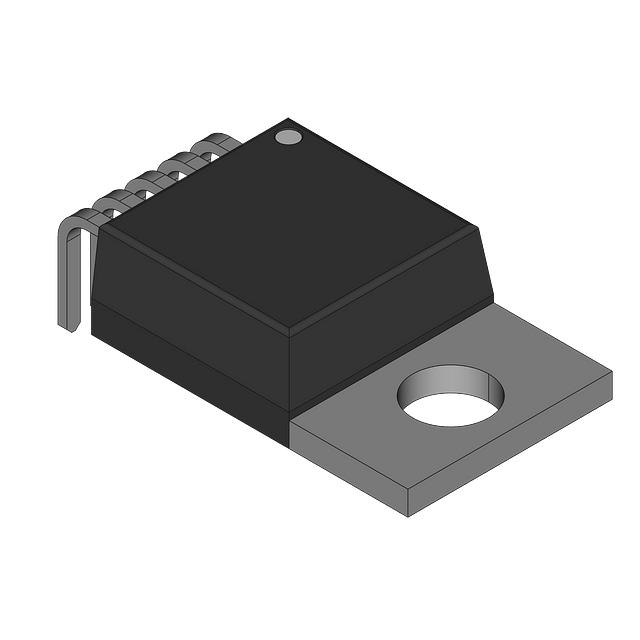
| package_case | TO-220-5 Formed Leads | 🔵 api | |
| supplier_device_package | TO-220-5 | 🔵 api |
When To Use
-
24V industrial/24V bus → 15.0V @ 3A: The LM2596T-5.0’s 40V maximum input voltage comfortably handles a 24V bus with margin for spikes and transients typical in industrial environments. Its 3A output current rating directly supports the 3A load without risking thermal or current-limit shutdown, whereas a part with lower current capability would enter thermal runaway or current foldback under full load.
-
12V automotive/battery rail → 10.0V @ 1.5A: The 4.5V minimum input rating and 40V maximum input cover typical automotive battery voltage swings and load-dump events. The fixed 5.0V output voltage can be adapted by adding an external resistor divider or choosing a different fixed version, but using this part directly for 10V would risk output regulation failure; however, for a 10V rail with a different part number, the LM2596T topology avoids shoot-through failure modes common in less rugged regulators.
-
4.5V–40V wide-input supply → 5.0V–15.0V @ 2.2A: The wide input voltage range and 3A max output current allow operation from a noisy, unregulated input rail down to a stable 5V or higher output. The fixed 5.0V output ensures stable regulation at the lower end; alternatives without the 40V input max would risk latch-up or damage from input surges beyond their voltage rating.
When Not To Use
-
High-efficiency designs requiring synchronous rectification: The LM2596T-5.0 is non-synchronous, meaning the external diode conduction causes higher losses at load, disqualifying it. Use a synchronous buck controller instead to avoid diode conduction losses and improve efficiency.
-
Output currents exceeding 3A: The 3A maximum output current rating limits its use in higher power applications. For loads above this rating, a multi-phase buck controller or high-current synchronous buck with external FETs is required to prevent device damage from overcurrent and thermal runaway.
-
Applications needing switching frequencies above 500kHz: The fixed 150kHz switching frequency cannot meet designs requiring small inductors or tight transient response at higher frequencies. Use a high-frequency buck controller for switching frequencies greater than 500kHz.
Application Notes
IC dissipates ≈3.3W at Vin=40V→Vout=10.0V @ 1.5A (η≈82%). This is IC loss only — the catch diode dissipates additional power. At elevated ambient, a heatsink is required for sustained operation above ~1.5A.
-
The switching node (SW) is the pin connected to the internal power switch and external inductor; minimize loop area around SW, the catch diode, and output capacitor to reduce EMI and ringing.
-
the GND pin and the Vin pin are noise-sensitive; ensure a low-inductance ground plane and decoupling capacitors close to Vin and GND pins to maintain stable input voltage and prevent voltage spikes.
-
Route the feedback pin (pin 2) away from SW and diode switching nodes to avoid noise coupling that can cause output voltage instability or oscillations.
-
The external diode must be a fast-recovery or Schottky type rated for at least 3A and 40V to prevent reverse recovery-induced voltage spikes.
Pin numbers are package-specific. Verify against the datasheet pinout diagram before routing.
Minimum External Components
Catch diode — Schottky, Vr ≥ 40V, If ≥ 3A Selection: Schottky forward recovery < 10ns vs 200–500ns for silicon. At 150kHz (period = 6.7µs), a 500ns-recovery diode is off for only 6.2µs before the next switch-on — it never fully turns off. Failure mode: Standard silicon rectifier: 200–500ns reverse recovery at 150kHz causes shoot-through current spikes every cycle — IC switch current exceeds rating, causing thermal runaway or immediate failure.
Output inductor — 68µH Selection: Isat ≥ 3.8A (peak current at max load). DCR < 100mΩ to limit conduction loss. At Vin=22V→Vout=15.0V: range is 33–68µH (30%→15% current ripple). Use 68µH for good regulation; 33µH acceptable if BOM cost is critical. Isat must be ≥ 3.8A — under-sizing Isat is the leading cause of field failures: the inductor saturates under peak current, spiking IC switch current beyond its rating. Failure mode: Isat below peak inductor current → core saturates → effective inductance collapses → switch current spikes beyond IC rating → thermal shutdown or permanent failure.
Input capacitor — ≥100µF electrolytic + 100nF ceramic (parallel) Selection: Electrolytic handles bulk ripple current; ceramic bypasses switching spikes. Voltage rating ≥ 40V with 20% margin. Failure mode: Insufficient input capacitance: supply rail collapses during switch-on current demand → output droops → erratic regulation and potential latch-up.
Output capacitor — ≥100µF electrolytic Selection: ESR < 200mΩ to keep output ripple below 50mVpp. Voltage rating ≥ 12V. Failure mode: High-ESR electrolytic: output ripple voltage = ESR × ΔIL. At 1A ripple and 500mΩ ESR → 500mVpp ripple — exceeds spec for virtually all loads.
Design Equations
Inductor sizing: At Vin=22V→Vout=15.0V: range is 33–68µH (30%→15% current ripple). Use 68µH for good regulation; 33µH acceptable if BOM cost is critical. Isat must be ≥ 3.8A — under-sizing Isat is the leading cause of field failures: the inductor saturates under peak current, spiking IC switch current beyond its rating.
Gotchas
-
[Mistake]: Using a standard rectifier diode instead of a fast-recovery or Schottky diode.
What happens: High reverse recovery time causes voltage spikes at the SW node, damaging the internal switch by exceeding its maximum voltage rating.
Fix: Use a diode with low reverse recovery time rated for at least 3A and 40V. -
[Mistake]: Operating above 3A output current without adequate heat sinking.
What happens: Junction temperature exceeds 125°C, triggering thermal shutdown or causing permanent device degradation due to thermal runaway.
Fix: Add a properly sized heatsink to the TO-220 package and verify thermal resistance to keep TJ below 125°C at maximum load. -
[Mistake]: Routing feedback trace near the SW node or diode cathode.
What happens: High-frequency switching noise couples into the feedback pin, causing output voltage ripple, instability, or oscillations.
Fix: Route feedback trace away from switching node and diode; use a separate ground return for feedback. -
[Mistake]: Assuming the fixed 5.0V output can be adjusted by adding a resistor divider on the output without considering device stability.
What happens: Incorrect feedback loading leads to improper regulation or oscillations, potentially damaging downstream circuitry.
Fix: Use a fixed version matching the output voltage requirement or a version with adjustable output and follow recommended compensation networks.