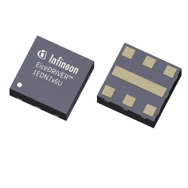
Key Specs
| Spec | Value | Condition | Source |
|---|---|---|---|
| Digikey Programmable | Not Verified | Digi-Key | |
| Driven Configuration | High-Side | Digi-Key | |
| Gate Type | GaN FET, MOSFET (N-Channel) | Digi-Key | |
| High Side Voltage Max Bootstrap | 200 V | Digi-Key | |
| Number Of Drivers | 1 | Digi-Key | |
| Package Case | - | Digi-Key | |
| Supplier Device Package | - | Digi-Key |
When To Use
-
High-side buck converter → 48V @ 5A: The 200 V max bootstrap voltage rating supports high-side operation well above 48V input rails, providing margin for load-dump and transient spikes. Using a synchronous buck controller without a high-side driver or with a lower bootstrap rating risks shoot-through or device failure on high-voltage rails.
-
GaN FET gate drive → 12V gate drive voltage: The integrated GaN FET N-Channel gate driver is optimized for fast switching and low gate charge at the required high-side voltage. A generic MOSFET driver lacking GaN optimization can cause excessive switching losses or incomplete gate drive, leading to thermal runaway.
-
Single-phase buck → 24V @ 10A peak load: The single driver channel suits single-phase topologies up to moderate current, avoiding complexity and cost of multi-phase controllers. A multi-phase buck controller would add unnecessary complexity and risk interphase shoot-through if not synchronized correctly.
When Not To Use
-
Output current requirement > 15A continuous: The single driver channel and lack of external FET control limit continuous current capability. Use a multi-phase buck controller to share current across multiple drivers and avoid thermal overstress.
-
Input voltage near or below output voltage (< 1V differential): The bootstrap high-side driver requires a voltage differential to operate properly; low dropout conditions cause driver malfunction. Use an LDO regulator for low-dropout and noise-sensitive applications.
-
Switching frequency > 500 kHz for compact magnetics: The part’s switching speed and gate drive are not specified for ultra-high frequency operation beyond 500 kHz, risking efficiency loss and excessive switching noise. Use a high-frequency buck controller designed for MHz-range switching.
Application Notes
-
The switching node (SW) must be routed with minimal parasitic inductance and capacitance to reduce voltage overshoot during hard switching transitions, especially critical due to GaN FET’s fast rise times.
-
Pins related to the high-side driver gate (not numbered here) are noise-sensitive; keep their traces short and shielded from noisy switching loops to prevent false triggering or erratic switching.
-
Ensure the bootstrap capacitor is placed physically close to the high-side driver supply pins to maintain stable gate drive voltage during switching cycles.
-
Implement a ground plane with guard rings around sensitive analog and gate driver return paths to minimize EMI coupling and ground bounce.
-
Avoid placing bulk output capacitors with high ESR close to the driver IC pins, as excessive ESR can cause instability and ringing in the gate drive signals.
Related Calculators
Use the MOSFET Power Loss Calculator to estimate losses in the MOSFETs driven by the 1EDN7116UXTSA1.
Gotchas
-
[Bootstrap voltage derating ignored]: Assuming the 200 V max bootstrap voltage applies continuously at all temperatures and duty cycles. In reality, the bootstrap rating may derate with temperature or high duty cycle, causing premature gate driver failure or latch-up. Fix: Verify bootstrap voltage derating curves in the datasheet at your operating point and design margin accordingly.
-
[High-side driver noise coupling]: Routing the gate driver return path through noisy switching current loops leads to erratic switching or oscillations not predicted by static load tests. Symptoms include jittery gate waveforms and increased EMI. Fix: Separate gate driver ground return from power ground and use Kelvin connections where possible.
-
[Minimum load requirement overlooked]: Operating with very light or no load can cause the driver to misbehave or the output voltage to overshoot due to insufficient conduction and feedback loop instability. Fix: Add a minimum load resistor or active load to ensure stable regulation at all times.
-
[Output capacitor ESR effect on gate drive stability]: Assuming any low-ESR output capacitor is acceptable, but very low ESR can cause gate drive ringing or instability due to LC tank effects with the GaN FET’s fast switching. Fix: Choose output capacitors with moderate ESR or add small series resistors on gate drive lines to damp oscillations.