Key Specs
| Spec | Value | Condition | Source |
|---|---|---|---|
| Function | Step-Down | [Digi-Key] | |
| Output Configuration | Positive | [Digi-Key] | |
| Topology | Buck | [Digi-Key] | |
| Output Type | Fixed | [Digi-Key] | |
| Number Of Outputs | 1 | [Digi-Key] | |
| Input Voltage (Min) | - | [Digi-Key] | |
| Input Voltage (Max) | 40V | [Digi-Key] | |
| Output Voltage (Min) | 5V | [Digi-Key] | |
| Output Voltage (Max) | - | [Digi-Key] | |
| Output Current (Max) | 3A | [Digi-Key] | |
| Switching Frequency (Typ) | 150kHz | [Digi-Key] | |
| Synchronous Rectifier | No | [Digi-Key] | |
| Operating Temperature Range | -40°C ~ 125°C (TA) | [Digi-Key] | |
| Mounting Type | Surface Mount | [Digi-Key] | |
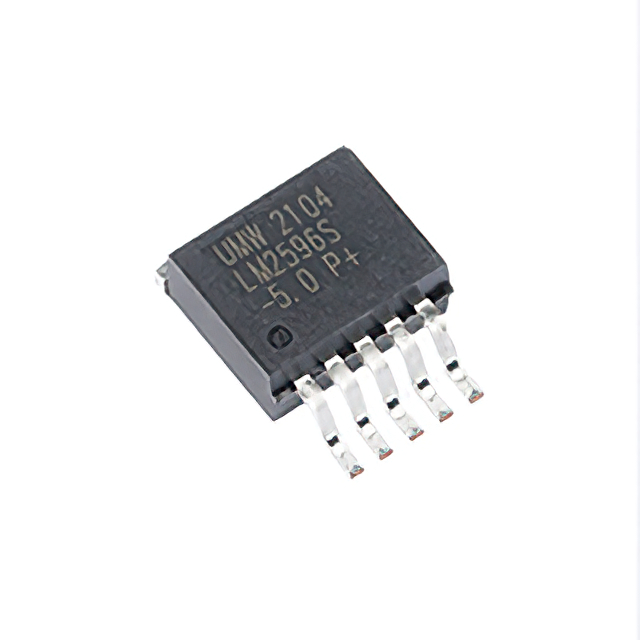
| Package Case | TO-263-6, D2PAK (5 Leads + Tab), TO-263BA | [Digi-Key] | |
| Supplier Device Package | TO-263-5L | [Digi-Key] |
When To Use
-
24V industrial supply → 5V @ 3A: The 40V maximum input rating covers common 24V rails with enough margin for transients. The fixed 5V output and 3A max load current suit standard logic and power domains without external feedback complexity. Using a synchronous buck controller here risks overdesign and higher BOM cost due to external FETs and control complexity.
-
Automotive accessory power from 12V battery → 5V @ 2.5A: The 40V max input voltage and internal switch rated for 4.5A peak current ensure handling load-dump and cold-crank surges safely without device destruction. A linear regulator would overheat quickly under these conditions, causing thermal shutdown or permanent damage.
-
Embedded system power rail from 36V nominal bus → 5V @ 1.5A: The 150kHz fixed internal oscillator frequency balances efficiency and size to maintain stable regulation with a moderate inductor size. An LDO regulator here would dissipate excessive power, leading to thermal runaway, while a high-frequency buck controller is unnecessary complexity for this load and voltage range.
When Not To Use
-
Output current > 3A continuous (e.g., 5V @ 5A): The 3A max output current rating is insufficient for this load. Use a high-current synchronous buck with external FETs to handle the increased current while maintaining efficiency and safe thermal margins.
-
Battery-powered IoT device needing ultra-low quiescent current: Typical standby current of 80µA is too high for long battery life in μA-level sleep modes. Use a low-IQ PFM buck regulator designed specifically for minimal standby current.
-
Input voltage above 40V (e.g., 48V telecom bus): The max input voltage rating of 40V limits operation on higher voltage rails. Use a multi-phase buck controller designed for high-voltage inputs and load sharing to avoid device latch-up or breakdown.
Application Notes
IC dissipates ≈3.3W at Vin=40V→Vout=10.0V @ 1.5A (η≈82%). This is IC loss only — the catch diode dissipates additional power. At elevated ambient, a heatsink is required for sustained operation above ~1.5A.
-
The switching node (SW) pin carries high di/dt and voltage spikes; keep its PCB copper area minimal and route away from sensitive analog traces to reduce EMI and ringing.
-
Feedback resistors (R1, R2) should be placed physically close to the IC pins with short, direct routing to the feedback pin to minimize noise pickup and maintain output voltage accuracy.
-
The ON/OFF pin must never exceed 25V; if input voltages or external signals risk going higher, add a resistor divider or clamp diode to protect this pin and prevent latch-up.
-
Input capacitors must have adequate voltage rating (≥40V) and RMS current rating to supply the instantaneous current at switch turn-on, preventing voltage transients that could cause erratic switching or damage.
-
Use a low ESR output capacitor meeting the minimum 22µF/V spec to ensure loop stability and prevent oscillations, especially under transient loads.
Minimum External Components
Catch diode — Schottky, Vr ≥ 40V, If ≥ 3A Selection: Schottky forward recovery < 10ns vs 200–500ns for silicon. At 150kHz (period = 6.7µs), a 500ns-recovery diode is off for only 6.2µs before the next switch-on — it never fully turns off. Failure mode: Standard silicon rectifier: 200–500ns reverse recovery at 150kHz causes shoot-through current spikes every cycle — IC switch current exceeds rating, causing thermal runaway or immediate failure.
Output inductor — 47µH Selection: Isat ≥ 3.8A (peak current at max load). DCR < 100mΩ to limit conduction loss. At Vin=20V→Vout=15.0V: range is 33–47µH (30%→15% current ripple). Use 47µH for good regulation; 33µH acceptable if BOM cost is critical. Isat must be ≥ 3.8A — under-sizing Isat is the leading cause of field failures: the inductor saturates under peak current, spiking IC switch current beyond its rating. Failure mode: Isat below peak inductor current → core saturates → effective inductance collapses → switch current spikes beyond IC rating → thermal shutdown or permanent failure.
Input capacitor — ≥100µF electrolytic + 100nF ceramic (parallel) Selection: Electrolytic handles bulk ripple current; ceramic bypasses switching spikes. Voltage rating ≥ 40V with 20% margin. Failure mode: Insufficient input capacitance: supply rail collapses during switch-on current demand → output droops → erratic regulation and potential latch-up.
Output capacitor — ≥100µF electrolytic Selection: ESR < 200mΩ to keep output ripple below 50mVpp. Voltage rating ≥ 12V. Failure mode: High-ESR electrolytic: output ripple voltage = ESR × ΔIL. At 1A ripple and 500mΩ ESR → 500mVpp ripple — exceeds spec for virtually all loads.
Design Equations
Inductor sizing: At Vin=20V→Vout=15.0V: range is 33–47µH (30%→15% current ripple). Use 47µH for good regulation; 33µH acceptable if BOM cost is critical. Isat must be ≥ 3.8A — under-sizing Isat is the leading cause of field failures: the inductor saturates under peak current, spiking IC switch current beyond its rating.
Gotchas
-
[Ignoring minimum output capacitor ESR requirements]: Designers may assume any 22µF capacitor suffices, but excessively low ESR ceramic capacitors can cause regulator instability and output voltage ringing. Symptom: output voltage oscillations or audible noise. Fix: Include a small ESR ceramic or a parallel polymer capacitor per datasheet recommendations to ensure stable operation.
-
[ON/OFF pin overvoltage from input rail]: Connecting the ON/OFF pin directly to the input rail above 25V or from a higher voltage source can cause permanent latch-up or device damage. Symptom: regulator fails to start or locks in an off state. Fix: Add a resistor divider or Zener clamp to keep ON/OFF pin voltage below 25V max.
-
[Startup with no load or very light load]: The internal feedback loop may not regulate properly at zero or near-zero load, causing output voltage overshoot or instability at startup. Symptom: output voltage spikes above 5.25V or erratic behavior on power-up. Fix: Ensure a minimum load of at least a few milliamps or add a bleed resistor on the output.
-
[Inadequate input capacitor RMS current rating]: Using input capacitors without sufficient RMS current rating leads to overheating and premature failure under continuous switching currents. Symptom: capacitor bulging, increased ESR, or input voltage ripple leading to regulator instability. Fix: Select input capacitors with RMS current rating exceeding expected switch currents per design equations.