Key Specs
| Spec | Value | Condition | Source |
|---|---|---|---|
| Current Continuous Drain ID 25 C | 66A (Tc) | Digi-Key | |
| Drain-source Voltage (Max) | 1200 V | Digi-Key | |
| Drive Voltage Max RDS On Min RDS On | 15V | Digi-Key | |
| FET Feature | - | Digi-Key | |
| FET Type | N-Channel | Digi-Key | |
| Gate Charge Qg Max VGS | 101 nC @ 15 V | Digi-Key | |
| Gate-source Voltage (Max) | +15V, -4V | Digi-Key | |
| Grade | - | Digi-Key | |
| Input Capacitance Ciss Max VDS | 2900 pF @ 1000 V | Digi-Key | |
| Mounting Type | Through Hole | Digi-Key | |
| Operating Temperature Range | -40°C ~ 175°C (TJ) | Digi-Key | |
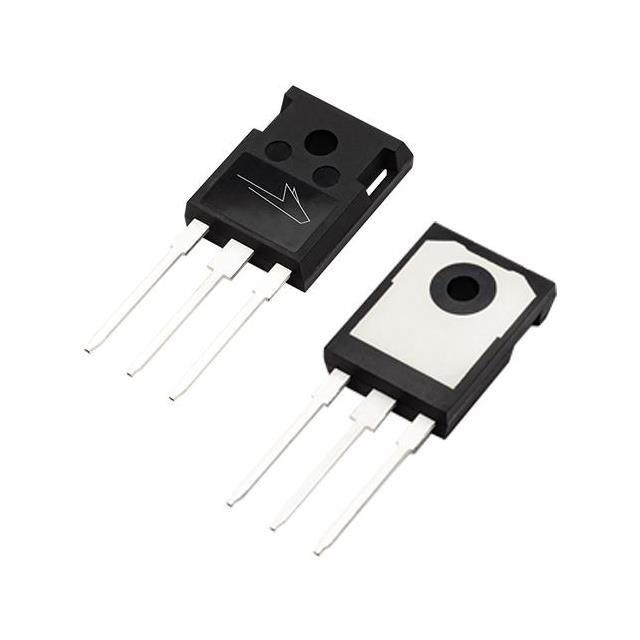
| Package Case | TO-247-3 | Digi-Key | |
| Power Dissipation (Max) | 326W (Tc) | Digi-Key | |
| Qualification | - | Digi-Key | |
| RDS On Max ID VGS | 53.5mOhm @ 33.3A, 15V | Digi-Key | |
| Supplier Device Package | TO-247-3 | Digi-Key | |
| Technology | SiCFET (Silicon Carbide) | Digi-Key | |
| VGS Th Max ID | 3.6V @ 9.5mA | Digi-Key |
When To Use
-
1200 V solar inverter front-end: The 1200 V drain-source voltage rating combined with a low typical R_DS(on) of 68 mΩ at 33.3 A allows the
C3M0040120Dto handle high-voltage DC input with efficient conduction losses. Using a lower-voltage MOSFET would risk avalanche or breakdown during PV string transients, causing catastrophic device failure. -
3-phase motor drive at 48 A peak: With a continuous drain current rating of 66 A at 25°C case temperature and a pulsed current max of 223 A, this device suits motor drive phases near 50 A. A synchronous buck controller with integrated FETs would not survive the 1200 V bus voltage, leading to shoot-through or latch-up during switching transitions.
-
High-voltage power factor correction (PFC) stage: The 1200 V rating and low switching energy (typical 950 µJ turn-on, 346 µJ turn-off) enable efficient hard-switching in boost PFC topologies working at several hundred volts DC bus. Using a silicon MOSFET or a lower-voltage device risks thermal runaway under high-frequency hard switching due to higher switching losses.
When Not To Use
-
Output current > 66 A continuous at ambient: The continuous drain current max of 66 A at 25°C case temperature limits sustained conduction. Use a multi-phase buck controller instead to parallel multiple devices and distribute current while maintaining thermal limits.
-
Efficiency-critical circuits requiring no diode losses: The body diode reverse recovery charge and current (typical 624 nC, 17 nC) contribute to switching losses and EMI. For zero external diode losses, use a synchronous buck controller with integrated synchronous rectification.
-
High-frequency switching > 500 kHz: The gate charge of 101 nC at 15 V and switching energies limit efficiency and switching speed. For switching frequencies above 500 kHz, use a high-frequency buck controller designed with lower gate charge devices optimized for fast transitions.
Application Notes
-
The switching node (SW) should have minimal parasitic inductance; keep the loop formed by the device drain, source, and external gate resistor as small as possible to reduce voltage overshoot and ringing during turn-on/off transitions.
-
the Gate pin and the Source pin are noise-sensitive; route gate drive traces away from high di/dt nodes and provide a low-inductance source connection for stable gate drive and to avoid false turn-on.
-
External gate resistor of approximately 2.5 Ω is recommended to balance switching speed and voltage overshoot; deviating significantly can cause excessive EMI or device stress.
-
Guard routing or ground plane segmentation is advised around the gate drive to prevent coupling from the switching node; ensure the gate driver return path is short and direct to minimize gate voltage oscillations.
-
The TO-247-3 package thermal interface must be properly mounted with a torque of at least 1 Nm to maintain low junction-to-case thermal resistance (0.46 °C/W); uneven mounting torque can increase thermal resistance, causing localized hotspots.
Gotchas
-
[Assuming max junction temperature = max continuous current rating at all ambient temperatures]: The 66 A continuous current rating is specified at 25 °C case temperature; at higher operating temperatures, effective current capability drops due to increased R_DS(on) and thermal limits. Without proper thermal derating curves, this leads to thermal runaway and device destruction.
Fix: Use detailed thermal derating graphs and measure junction temperature under worst-case conditions, ensuring operation well below max TJ of 175 °C. -
[Neglecting gate voltage transient limits during switching]: The device maximum transient gate-source voltage is ±19 V, yet typical drive voltage is ±15 V. Overshoot due to ringing or gate driver supply spikes can exceed this, causing gate oxide stress and latent damage.
Fix: Include gate voltage clamping (e.g., TVS diode or zener clamp) and carefully control gate driver supply to prevent voltage excursions beyond ±15 V nominal. -
[Misinterpreting diode forward voltage specs under temperature]: The diode forward voltage varies significantly (typical 4.9 V at 175 °C vs. 5.5 V at 25 °C). Designs using fixed voltage drops for current sensing or protection may malfunction in high-temperature operation, causing false triggering or misestimation of losses.
Fix: Characterize diode forward voltage across the full operating temperature range and include temperature compensation in control algorithms. -
[Switching node layout causing erratic reverse recovery behavior]: Excessive parasitic inductance in the drain-source loop can amplify reverse recovery current spikes (typical reverse recovery charge 624 nC), causing voltage overshoot and EMI bursts not predicted by static datasheet values.
Fix: Minimize parasitic inductances by placing the device close to the DC bus and output capacitor, and use low-inductance bus bars or PCBs optimized for high di/dt switching.