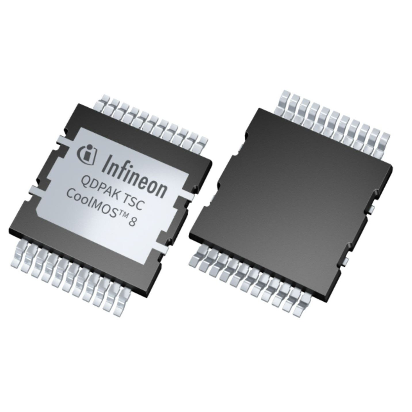
Key Specs
| Spec | Value | Condition | Source |
|---|---|---|---|
| Current Continuous Drain ID 25 C | 116A (Tc) | Digi-Key | |
| Drain-source Voltage (Max) | 1200 V | Digi-Key | |
| Drive Voltage Max RDS On Min RDS On | 18V, 20V | Digi-Key | |
| FET Feature | - | Digi-Key | |
| FET Type | N-Channel | Digi-Key | |
| Gate Charge Qg Max VGS | 82 nC @ 20 V | Digi-Key | |
| Gate-source Voltage (Max) | +25V, -10V | Digi-Key | |
| Grade | Automotive | Digi-Key | |
| Input Capacitance Ciss Max VDS | 2667 pF @ 800 V | Digi-Key | |
| Mounting Type | Surface Mount | Digi-Key | |
| Operating Temperature Range | -55°C ~ 175°C (TJ) | Digi-Key | |
| Package Case | 22-PowerBSOP Module | Digi-Key | |
| Power Dissipation (Max) | 577W (Tc) | Digi-Key | |
| Qualification | AEC-Q101 | Digi-Key | |
| RDS On Max ID VGS | 25mOhm @ 43A, 20V | Digi-Key | |
| Supplier Device Package | PG-HDSOP-22 | Digi-Key | |
| Technology | SiCFET (Silicon Carbide) | Digi-Key | |
| VGS Th Max ID | 5.1V @ 13.7mA | Digi-Key |
When To Use
-
1200 V industrial motor drive @ 50A: The 1200 V drain-source voltage max and 116A continuous current rating at Tc make this part suitable for high-voltage motor drives with transient voltage spikes. Using a synchronous buck controller with lower voltage rating risks avalanche or latch-up from inductive load kickback.
-
Automotive onboard charger @ 20V drive, 40A: The automotive grade and gate charge of 82 nC at 20 V drive voltage enable reliable switching at automotive temperatures and speeds. A multi-phase buck controller with lower gate voltage margin could suffer shoot-through or excessive losses under transient load steps.
-
High-temperature industrial power supply @ 100A continuous: The 175°C maximum junction temperature rating supports operation in harsh environments without thermal runaway. An LDO regulator or standard MOSFET without SiC technology would experience rapid thermal degradation or catastrophic failure beyond 150°C.
When Not To Use
-
Output current > 116A continuous: The 116A continuous drain current at Tc limits maximum load current. Use a multi-phase buck controller to distribute current across multiple FETs and avoid thermal and electrical overstress.
-
Switching frequency > 500 kHz: Although gate charge is moderate, the 82 nC at 20 V limits feasible switching speed due to gate drive losses and thermal buildup. Use a high-frequency buck controller optimized for MHz-range operation.
-
Input-output voltage differential < 1V with noise-sensitive load: The SiC MOSFET’s switching noise and threshold voltage variation are unsuitable for low dropout linear regulation. Use an LDO regulator for low noise and tight voltage regulation in this regime.
Related Calculators
Use the MOSFET Power Loss Calculator to estimate conduction and switching losses for the AIMCQ120R020M1TXTMA1 in your SiC inverter or power stage design.
Application Notes
-
The switching node (SW) must be routed with a low-inductance, wide copper area to handle high di/dt and minimize voltage overshoot; poor SW layout can induce ringing and gate drive stress.
-
Pins 4 and the gate and source pin are noise-sensitive; ensure short, low-impedance gate drive loops and use local gate resistors to damp parasitic oscillations.
-
Guard routing around the drain pins (high voltage) is recommended to prevent creepage and corona discharge, especially in automotive environments.
-
The negative gate-source voltage rating is -10V max; do not exceed this during negative transients on the gate drive, or risk gate oxide damage.
-
Input capacitance (Ciss) is 2667 pF at 800 V, which impacts switching loss and EMI; verify gate driver capability and EMI filtering accordingly.
Gotchas
-
[Gate drive negative voltage underestimation]: Engineers may assume the gate-source voltage rating only limits positive voltage, neglecting the -10V negative rating. Negative switching spikes or gate driver undershoot can puncture the gate oxide, causing latent degradation. Fix: Use a gate driver with negative voltage clamping or add a gate-to-source Zener diode clamp.
-
[Thermal derating at high junction temperature]: The continuous current rating of 116A is specified at Tc, not junction temperature. Operating near 175°C junction without proper thermal management causes rapid Rds(on) increase and thermal runaway. Fix: Verify junction temperature with thermal simulation and ensure adequate heat sinking to keep TJ below rated max.
-
[Switching node layout causing oscillations]: Excessive loop inductance on the SW node can couple into the gate drive loop, causing high-frequency oscillations that lead to erratic gate voltage and increased EMI. Fix: Minimize loop area by placing gate driver close to FET and use Kelvin source connections.
-
[Minimum load requirement ignored in synchronous operation]: In synchronous buck topologies, running below a minimum load can cause shoot-through or negative inductor current, stressing the device. Fix: Include a minimum load or use synchronous controller features that prevent reverse conduction.