Key Specs
| Spec | Value | Condition | Source |
|---|---|---|---|
| Channel Type | 3-Phase | Digi-Key | |
| Current Peak Output Source Sink | 1.5A, 1.5A | Digi-Key | |
| Digikey Programmable | Not Verified | Digi-Key | |
| Driven Configuration | Half-Bridge | Digi-Key | |
| Gate Type | MOSFET (N-Channel) | Digi-Key | |
| Input Type | Non-Inverting | Digi-Key | |
| Logic Voltage Vil Vih | 0.8V, 2V | Digi-Key | |
| Mounting Type | Surface Mount | Digi-Key | |
| Number Of Drivers | 3 | Digi-Key | |
| Operating Temperature Range | -40°C ~ 125°C (TJ) | Digi-Key | |
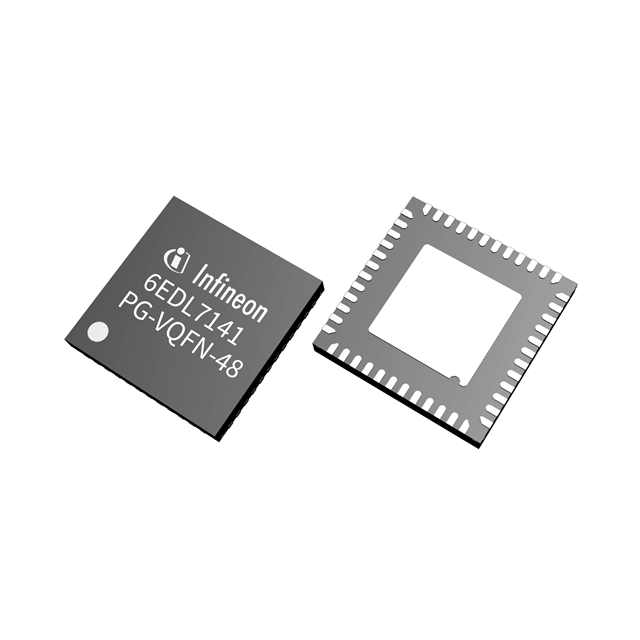
| Package Case | 48-VFQFN Exposed Pad | Digi-Key | |
| Rise Fall Time (Typ) | - | Digi-Key | |
| Supplier Device Package | PG-VQFN-48-78 | Digi-Key | |
| Voltage Supply | 5.5V ~ 60V | Digi-Key |
When To Use
Use the 6EDL7141XUMA1 in 3-phase motor control applications requiring half-bridge MOSFET drivers with peak output currents of 1.5A source and sink. It is well suited for surface-mount designs operating within a wide supply voltage range of 5.5V to 60V and junction temperatures from -40°C to 125°C. Ideal applications include industrial drives and inverter stages where non-inverting logic inputs and fast switching MOSFET gate drive are required.
When Not To Use
Do not use the 6EDL7141XUMA1 in applications requiring full-bridge driver configurations or peak output currents exceeding 1.5A. For single-channel or isolated gate drivers, or where programmable logic input thresholds are essential, consider alternative devices with those specific features. Avoid this part in designs needing logic voltage thresholds outside 0.8V (VIL) and 2V (VIH).
Application Notes
The switching node connected to the MOSFET gates must have the smallest possible loop area to minimize parasitic inductances and reduce EMI and voltage overshoot. The logic input pins are noise-sensitive; use proper filtering and routing to prevent false triggering. Given the peak output current of 1.5A and operating temperature up to 125°C junction, a thermal management strategy including a well-designed PCB copper area and the exposed pad package is sufficient; an additional heatsink is generally not required under typical operating conditions.
Gotchas
-
Ignoring proper bootstrap capacitor selection:
Engineers sometimes omit or undersize the bootstrap capacitor, resulting in insufficient voltage on the high-side driver supply. This causes incomplete MOSFET turn-on, increased conduction losses, and potential overheating. Always use a low-ESR capacitor rated for the supply voltage and verify the bootstrap voltage during operation. -
Neglecting gate resistor optimization:
Using either no gate resistor or an excessively low value can lead to high di/dt and dv/dt, causing EMI, voltage ringing, and possible damage to the MOSFET or driver. Conversely, overly large gate resistors increase switching losses and slow response. Select gate resistors based on MOSFET gate charge and switching speed requirements to balance EMI and efficiency. -
Incorrect logic input voltage levels:
Applying input signals outside the specified logic voltage thresholds (VIL = 0.8V, VIH = 2V) can cause unpredictable driver behavior or failure to switch. Ensure control signals meet these thresholds or use level-shifting circuitry.