Key Specs
| Spec | Value | Condition | Source |
|---|---|---|---|
| Channel Type | Independent | Digi-Key | |
| Current Peak Output Source Sink | 5A, 5A | Digi-Key | |
| Digikey Programmable | Not Verified | Digi-Key | |
| Driven Configuration | Low-Side | Digi-Key | |
| Gate Type | GaN FET, MOSFET (N-Channel) | Digi-Key | |
| High Side Voltage Max Bootstrap | 20 V | Digi-Key | |
| Input Type | Non-Inverting | Digi-Key | |
| Logic Voltage Vil Vih | - | Digi-Key | |
| Mounting Type | Surface Mount | Digi-Key | |
| Number Of Drivers | 2 | Digi-Key | |
| Operating Temperature Range | -40°C ~ 150°C (TJ) | Digi-Key | |
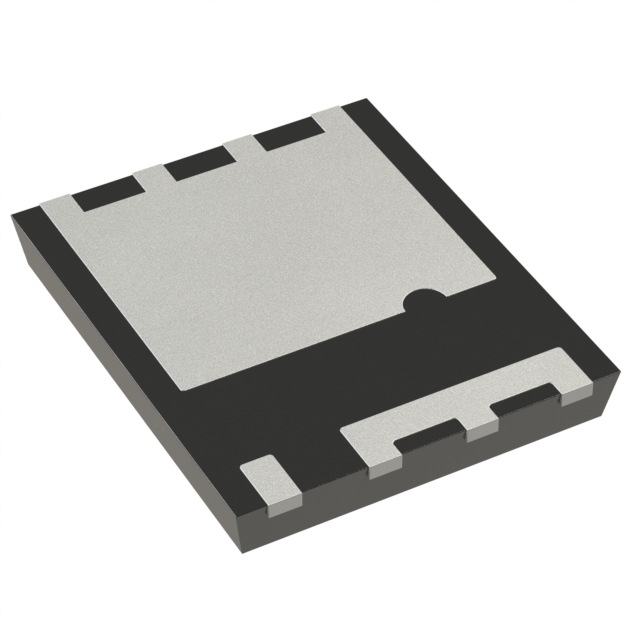
| Package Case | 8-WDFN Exposed Pad | Digi-Key | |
| Rise Fall Time (Typ) | 5.3ns, 4.5ns | Digi-Key | |
| Supplier Device Package | PG-WSON-8-1 | Digi-Key | |
| Voltage Supply | 4.5V ~ 20V | Digi-Key |
When To Use
-
Dual-channel synchronous buck for server VRM @ 5A: The 2EDN7524GXTMA1’s matched channel-to-channel delay of 1ns typical ensures tight timing control for interleaved or dual-phase synchronous buck stages, minimizing cross-conduction and shoot-through. A generic dual driver without this delay matching would risk increased switching losses and potential thermal runaway from uneven switching of phases.
-
GaN FET gate driver in telecom SMPS @ 20V supply: Supporting a maximum operating voltage of 20V and sourcing/sinking 5A peak current makes this device ideal for driving GaN or logic-level MOSFETs with fast rise/fall times (typical 5–6.5ns). Using a driver with lower peak current capability risks insufficient gate drive, causing slow switching, increased losses, and device overheating.
-
High-frequency isolated LLC converter with bootstrap supply: The integrated bootstrap capability up to 20V and independent low-side channel configuration suits LLC topologies with bootstrap-powered high-side MOSFETs. Controllers missing this bootstrap voltage range or independent channels may suffer from latch-up or incomplete gate drive during zero-voltage switching intervals.
When Not To Use
-
Output current exceeding 5A per channel: The max source/sink current rating is 5A typical. For loads above this, use a high-current synchronous buck with external FETs to handle the higher current while maintaining efficiency and avoiding driver damage.
-
Switching frequency above 500 kHz: The part’s rise/fall times and propagation delays (typical ~20–25 ns) limit suitability for very high-frequency operation. For switching frequencies > 500 kHz, use a high-frequency buck controller designed for ultrafast gate drive and minimal delay.
-
Low-voltage dropout applications with tight output noise requirements: Since the device is a gate driver and not a linear regulator, it cannot regulate low dropout or provide low noise output voltage. Use an LDO regulator when input-output voltage differential is < 1V and noise is critical.
Application Notes
-
Keep the SW node loop area minimal to reduce EMI; the driver’s fast 5.3–6.5 ns rise/fall times exacerbate high dv/dt switching noise. Place gate and source return paths close.
-
Pins INA and INB (input signals) are noise-sensitive with input thresholds around 2.5 V typical for switching on; route their traces away from noisy switching nodes and use local decoupling to prevent false triggering.
-
Enable pins ENA and ENB have internal pull-down resistors (~100 kΩ); ensure these pins are driven actively or tied to GND to avoid floating states that cause erratic output switching.
-
The device supports multiple package types (DSO-8, TSSOP-8, WSON-8) with varying thermal resistances; select package and PCB copper area according to power dissipation requirements for stable junction temperature.
-
Guard routing around gate drive traces is recommended to minimize cross-talk between channels, especially when operating at high switching speeds or in multi-phase applications.
Gotchas
-
[Bootstrap voltage margin underestimated]: Designers may assume the max bootstrap voltage of 20V covers all supply variations, but transient overshoot or ringing above this can cause gate driver latch-up or permanent damage. Symptom: erratic high-side switching or device failure under startup transient. Fix: measure bootstrap voltage waveform with high bandwidth scope and include clamping or snubber circuits if overshoot exceeds 20V.
-
[Input signal pulse width too narrow]: The minimum input pulse width is 151 ns; shorter pulses pass simulation but cause incomplete gate drive, leading to partial MOSFET switching and high losses. Symptom: distorted output waveform and excessive device heating. Fix: verify input pulse widths exceed minimum and add input conditioning or pulse stretching if needed.
-
[Thermal performance mismatch due to package choice]: Using the DSO-8 package without adequate PCB thermal relief can push junction-to-board thermal resistance above 16 K/W typical, causing junction temperature to rise unexpectedly. Symptom: thermal derating, reduced reliability, or thermal shutdown during continuous operation. Fix: verify thermal resistance with actual PCB layout, consider WSON-8 package for better heat dissipation.
-
[Floating enable pins causing output glitching]: Assuming ENA/ENB pins can be left unconnected leads to the internal 100 kΩ pull-down being insufficient to prevent output switching noise or false turn-on. Symptom: output gate toggling at low-level input noise or startup glitches. Fix: tie enable pins to defined logic levels with low impedance or drive actively.