Key Specs
| Spec | Value | Condition | Source |
|---|---|---|---|
| Current Continuous Drain ID 25 C | 33A (Tc) | Digi-Key | |
| Drain-source Voltage (Max) | 1200 V | Digi-Key | |
| Drive Voltage Max RDS On Min RDS On | 12V | Digi-Key | |
| FET Feature | - | Digi-Key | |
| FET Type | N-Channel | Digi-Key | |
| Gate Charge Qg Max VGS | 51 nC @ 15 V | Digi-Key | |
| Gate-source Voltage (Max) | ±25V | Digi-Key | |
| Grade | - | Digi-Key | |
| Input Capacitance Ciss Max VDS | 1500 pF @ 100 V | Digi-Key | |
| Mounting Type | Through Hole | Digi-Key | |
| Operating Temperature Range | -55°C ~ 175°C (TJ) | Digi-Key | |
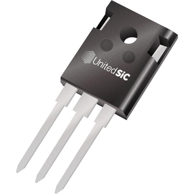
| Package Case | TO-247-3 | Digi-Key | |
| Power Dissipation (Max) | 254.2W (Tc) | Digi-Key | |
| Qualification | - | Digi-Key | |
| RDS On Max ID VGS | 100mOhm @ 20A, 12V | Digi-Key | |
| Supplier Device Package | TO-247-3 | Digi-Key | |
| Technology | SiCFET (Cascode SiCJFET) | Digi-Key | |
| VGS Th Max ID | 6V @ 10mA | Digi-Key |
When To Use
-
1200V industrial motor drive → 600V @ 20A: The 1200 V rating with 33A continuous drain current at 25°C ensures robust operation under high-voltage motor bus conditions with ample margin. Using a lower-voltage MOSFET risks avalanche or punch-through breakdown during motor startup transients, causing device failure.
-
High-voltage solar inverter stage → 400V @ 30A: The SiCFET cascode architecture with 100mΩ RDS(on) at 20A and 12 V drive balances conduction losses and high-voltage withstand, enabling efficient switching at high currents. A standard silicon MOSFET would suffer from thermal runaway due to higher gate charge and slower switching.
-
Industrial power supply primary switch → 1200V @ 10A: The ±25 V maximum gate-source rating combined with a 51 nC gate charge at 15 V allows stable gate drive with common gate drivers without overstressing the gate oxide. Using a device with lower gate voltage tolerance risks gate oxide damage during driver overshoot or ringing, causing early latch-up or short.
When Not To Use
-
>33A continuous output current: The maximum continuous drain current of 33A at 25°C is insufficient for loads exceeding this. Use a multi-phase buck controller with parallel FETs or higher-rated devices to avoid thermal runaway and device destruction.
-
Switching frequency > 500 kHz for compact magnetics: The gate charge of 51 nC at 15 V and input capacitance of 1500 pF limit switching speed and increase switching losses at high frequencies. Use a high-frequency buck controller designed for low gate charge FETs to prevent excessive switching losses and thermal stress.
-
Input-output voltage differential < 1 V, noise-sensitive analog rail: This device’s RDS(on) and switching nature cause noise unsuitable for low dropout linear regulation or sensitive analog loads. Use an LDO regulator instead to maintain low noise and tight voltage regulation.
Application Notes
-
The switching node (SW) sees high dv/dt and must be routed with minimum loop area to reduce EMI; place the device close to the driver and minimize PCB parasitic inductance.
-
the Gate pin, 2 (Drain), and the Source pin are the three leads; the gate drive requires a clean low-inductance path with a dedicated gate resistor to damp oscillations due to the 51 nC gate charge.
-
Because the device is a SiCFET cascode, careful gate drive voltage control within ±25 V is critical; transient overvoltage spikes on the gate line can cause irreversible damage.
-
Guard routing or ground plane isolation is recommended around the gate pin to reduce capacitive coupling from the drain switching node and avoid false triggering.
-
Mount the device on a heatsink or copper area rated for at least 254.2 W power dissipation at Tc to maintain junction temperature below 175°C during continuous operation.
Gotchas
-
[Underestimating thermal derating at elevated junction temperature]: The continuous drain current of 33A is rated at 25°C case temperature; as junction temperature approaches 175°C, the safe current drops significantly, causing thermal runaway if load current is kept constant.
Fix: Measure case temperature under worst-case load and apply derating curves from the datasheet before finalizing current ratings. -
[Gate drive ringing due to high input capacitance and fast switching]: The 1500 pF input capacitance combined with 51 nC gate charge causes oscillations if gate resistor and layout inductance are not optimized, resulting in gate voltage overshoot beyond ±25 V limits and device failure.
Fix: Use a small series gate resistor (e.g., 3–10 Ω) and minimize gate loop inductance; verify gate voltage waveform with a high-bandwidth probe. -
[Floating source pin during certain topologies]: In topologies where the source node is not continuously referenced to ground during switching (e.g., half-bridge), gate drive referencing can shift, causing threshold variation and erratic switching.
Fix: Ensure the gate drive stage references the source correctly with a low-impedance connection; consider bootstrap or isolated gate drivers if topology demands. -
[Startup without minimum load causing oscillations]: At light or no load, the device can enter unintended oscillation due to the interaction of device capacitances and external components, leading to audible noise or output voltage ripple.
Fix: Add a minimum load resistor or active load to stabilize operation during startup and light load conditions.