Key Specs
| Spec | Value | Condition | Source |
|---|---|---|---|
| Current Continuous Drain ID 25 C | 54A (Tc) | Digi-Key | |
| Drain-source Voltage (Max) | 1200 V | Digi-Key | |
| Drive Voltage Max RDS On Min RDS On | 18V | Digi-Key | |
| FET Feature | - | Digi-Key | |
| FET Type | N-Channel | Digi-Key | |
| Gate Charge Qg Max VGS | 75 nC @ 18 V | Digi-Key | |
| Gate-source Voltage (Max) | +22V, -10V | Digi-Key | |
| Grade | - | Digi-Key | |
| Input Capacitance Ciss Max VDS | 1700 pF @ 800 V | Digi-Key | |
| Mounting Type | Through Hole | Digi-Key | |
| Operating Temperature Range | -55°C ~ 175°C (TJ) | Digi-Key | |
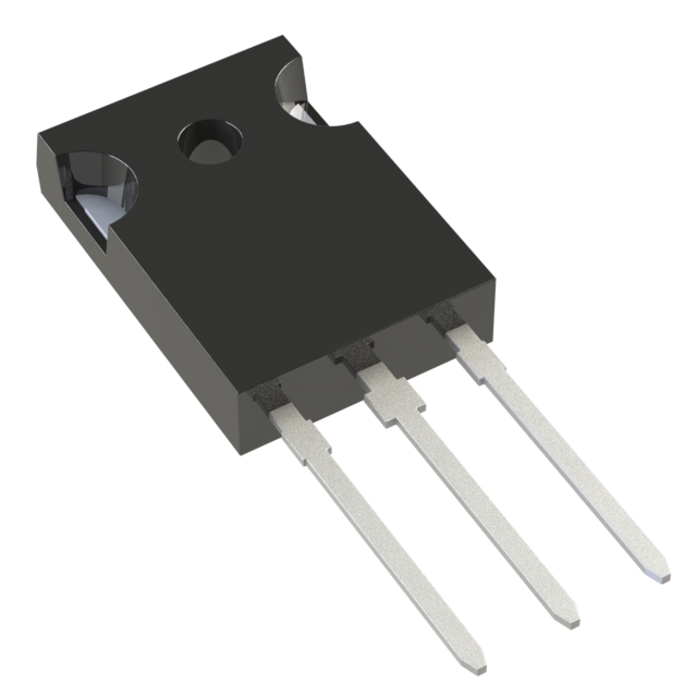
| Package Case | TO-247-3 | Digi-Key | |
| Power Dissipation (Max) | 231W (Tc) | Digi-Key | |
| Qualification | - | Digi-Key | |
| RDS On Max ID VGS | 54mOhm @ 20A, 18V | Digi-Key | |
| Supplier Device Package | TO-247-3 | Digi-Key | |
| Technology | SiCFET (Silicon Carbide) | Digi-Key | |
| VGS Th Max ID | 4.4V @ 10mA | Digi-Key |
When To Use
Use the NTHL040N120M3S in high-voltage, high-current power conversion applications such as industrial motor drives, solar inverters, and power supplies requiring a blocking voltage of up to 1200 V and continuous drain current of 54 A (Tc). Its low Rds(on) of 54 mΩ at 20 A and 18 V gate drive voltage makes it well-suited for efficient switching in hard-switching topologies. The SiCFET technology enables operation at elevated junction temperatures up to 175°C, making it ideal for environments with high thermal stress.
When Not To Use
Do not use the NTHL040N120M3S in low-voltage (< 600 V) or low-current (< 10 A) applications where the relatively high Rds(on) and gate charge (75 nC @ 18 V) would result in inefficient switching losses; in such cases, a MOSFET with lower gate charge and Rds(on) optimized for low-voltage operation is preferable. Also avoid this device in applications requiring fast switching at gate voltages below 18 V, as the Rds(on) and threshold voltage characteristics are specified at 18 V gate drive.
Application Notes
When using the NTHL040N120M3S, the drain node switches at high voltage and must be routed with minimal loop area to reduce parasitic inductance and voltage overshoot. The gate pin is noise-sensitive and should be driven by a low-impedance gate driver with a short connection path to minimize gate ringing and false triggering. Due to the maximum power dissipation of 231 W (Tc), a properly sized heatsink is necessary at typical operating currents of 54 A to maintain junction temperatures within the -55°C to 175°C range. Careful layout and thermal design ensure reliable operation and maximize device lifetime.
Gotchas
-
Gate Overvoltage:
- Mistake: Applying gate-source voltage exceeding +22 V or below -10 V during transient conditions.
- Failure Mode: Permanent damage to the gate oxide leading to device failure.
- Fix: Use gate drivers with voltage clamping or level shifting to ensure gate voltage stays within specified limits.
-
Insufficient Thermal Management:
- Mistake: Operating the device at high current (close to 54 A) without an adequate heatsink.
- Failure Mode: Junction temperature exceeds 175°C, causing device degradation or catastrophic failure.
- Fix: Design for proper heat sinking and verify thermal resistance from junction to case; monitor temperature during operation.
-
Excessive Switching Loop Inductance:
- Mistake: Long PCB traces and large loop areas on the drain switching node.
- Failure Mode: Voltage overshoot exceeding 1200 V rating, leading to avalanche breakdown.
- Fix: Minimize loop area, use proper snubber circuits, and employ careful PCB layout techniques.