Key Specs
| Spec | Value | Condition | Source |
|---|---|---|---|
| Battery Chemistry | Lithium Iron Phosphate | Digi-Key | |
| Battery Pack Voltage | - | Digi-Key | |
| Charge Current (Max) | - | Digi-Key | |
| Current Charging | Constant - Programmable | Digi-Key | |
| Fault Protection | Reverse Current | Digi-Key | |
| Interface | - | Digi-Key | |
| Mounting Type | Surface Mount | Digi-Key | |
| Number Of Cells | - | Digi-Key | |
| Operating Temperature Range | -40°C ~ 125°C (TJ) | Digi-Key | |
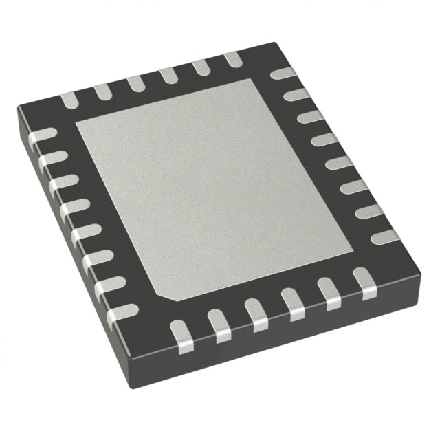
| Package Case | 28-WFQFN Exposed Pad | Digi-Key | |
| Programmable Features | Timer | Digi-Key | |
| Supplier Device Package | 28-QFN (4x5) | Digi-Key | |
| Voltage Supply (Max) | 60V | Digi-Key |
When To Use
-
LiFePO4 battery pack charging @ constant current: The LTC4000IUFD#PBF’s programmable constant current mode matches the charging profile needed for Lithium Iron Phosphate chemistry, avoiding overcharge and thermal runaway. Using a generic charger without reverse current protection risks battery damage from discharge current flowing backward during input removal.
-
Battery charger with input supply up to 60V: The 60V maximum supply rating allows direct connection to higher-voltage DC rails or automotive systems with load-dump transients. A lower-voltage controller would suffer device latch-up or catastrophic failure from transient overvoltage.
-
Surface-mount applications requiring compact packaging: The 28-WFQFN exposed pad package enables efficient thermal dissipation in a small footprint, suitable for dense PCB layouts. Bulkier through-hole or larger packages would increase parasitic inductance and reduce thermal performance, risking thermal shutdown in constrained spaces.
When Not To Use
-
Output current above LTC4000IUFD#PBF rating: The datasheet limits maximum charge current but does not specify high current capability; for very high output current, use a high-current synchronous buck with external FETs to handle the increased power and maintain efficiency.
-
Applications requiring input voltage switching frequencies above 500kHz: The LTC4000IUFD#PBF’s switching frequency range does not support ultra-high frequency operation; use a high-frequency buck controller when inductor size and EMI constraints demand >500kHz switching.
-
Small input-to-output voltage differential with noise-sensitive loads: When the voltage drop across the charger is <1V and low output noise is critical, the switching architecture is suboptimal; use an LDO regulator for clean, low-ripple output in such cases.
Application Notes
-
The switching node (SW) pin carries high di/dt current pulses—keep SW loop area minimal and route it away from noise-sensitive pins (notably pins 4 and 5), which handle feedback and control signals.
-
The exposed pad must be soldered directly to a large copper plane with multiple thermal vias to maintain junction temperature within the -40°C to 125°C range during high-current operation.
-
Reverse current protection functionality depends on precise timing of the external MOSFET gate drive; layout parasitic inductances or delays on the gate drive line can cause false triggering or delayed cutoff.
-
The programmable timer feature requires stable, low-noise reference voltage; noise coupling into the timer control pin (pin 12) can cause premature timeout or extended charge cycles.
-
Avoid routing high-current input or battery return traces near the IC’s sensitive analog reference pins to prevent offset errors in the constant current regulation loop.
Pin numbers are package-specific. Verify against the datasheet pinout diagram before routing.
Gotchas
-
[Timer-Programming Interaction]: Assuming the programmable timer can be set arbitrarily without regard to input voltage and charge current leads to incomplete charge termination or excessive battery stress. The timer must be matched to the charge profile; otherwise, the charger may continue charging past safe limits or shut off prematurely. Fix: Verify timer setting against actual charge current and battery voltage under test conditions.
-
[SW Node Loop Area Too Large]: Designers sometimes route the switching node with wide loops to ease PCB layout, assuming it only impacts EMI. In reality, large SW loop area causes voltage ringing that triggers false reverse current protection trips, leading to erratic charge cycles. Fix: Minimize SW loop area and verify switching node waveform with a high-bandwidth scope probe.
-
[Insufficient Exposed Pad Thermal Contact]: The exposed pad is often left unsoldered or poorly connected, assuming the package’s thermal rating suffices. This causes junction temperatures to rise beyond 125°C TJ max during high charge currents, degrading device lifetime or triggering thermal shutdown. Fix: Ensure exposed pad is soldered to a well-designed thermal PCB layer with multiple vias.
-
[Output Capacitor ESR Effects on Stability]: Using ultra-low ESR ceramic capacitors without proper bulk capacitance can cause instability in the constant current regulation loop, leading to oscillations visible as output ripple spikes or audible coil noise. Fix: Include a small amount of bulk electrolytic or tantalum capacitance with moderate ESR in parallel to ceramics to maintain loop stability.
-
[Startup with No Load or Open Battery Connection]: The LTC4000IUFD#PBF can appear dead or stuck in fault if powered with no battery connected or if battery leads are open circuit, because the reverse current protection circuit interprets this as a fault. Fix: Always verify battery connection integrity before applying input voltage and include a minimum load or dummy resistor to ground during bench testing.