Key Specs
| Spec | Value | Condition | Source |
|---|---|---|---|
| Current Continuous Drain ID 25 C | 30A (Tc) | Digi-Key | |
| Drain-source Voltage (Max) | 1200 V | Digi-Key | |
| Drive Voltage Max RDS On Min RDS On | 15V | Digi-Key | |
| FET Feature | - | Digi-Key | |
| FET Type | N-Channel | Digi-Key | |
| Gate Charge Qg Max VGS | 51 nC @ 15 V | Digi-Key | |
| Gate-source Voltage (Max) | +19V, -8V | Digi-Key | |
| Grade | - | Digi-Key | |
| Input Capacitance Ciss Max VDS | 1350 pF @ 1000 V | Digi-Key | |
| Mounting Type | Through Hole | Digi-Key | |
| Operating Temperature Range | -55°C ~ 150°C (TJ) | Digi-Key | |
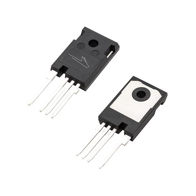
| Package Case | TO-247-4 | Digi-Key | |
| Power Dissipation (Max) | 113.6W (Tc) | Digi-Key | |
| Qualification | - | Digi-Key | |
| RDS On Max ID VGS | 90mOhm @ 20A, 15V | Digi-Key | |
| Supplier Device Package | TO-247-4L | Digi-Key | |
| Technology | SiCFET (Silicon Carbide) | Digi-Key | |
| VGS Th Max ID | 4V @ 5mA | Digi-Key |
When To Use
-
1200 V DC Bus → 48 V @ 20 A: The 1200 V drain-source rating with a robust 30 A continuous current at 25°C junction temperature makes this part ideal for high-voltage bus conversion without risking avalanche or breakdown. Lower-voltage MOSFETs would fail by overstress during bus transients or load dump, causing destructive avalanche and permanent damage.
-
Industrial Motor Drive Phase Leg at 15 V Gate Drive: The combination of a 15 V recommended drive voltage and a maximum Rds(on) of 90 mΩ at 20 A ensures efficient conduction and low switching losses in gate driver topologies limited to 15 V PWM signals. Using devices rated only at 10 V gate drive risks incomplete enhancement, causing excessive conduction losses and thermal runaway under continuous high current.
-
High-Temperature Power Stage Operating to 150°C TJ: The extended junction temperature rating up to 150°C supports harsh industrial environments without premature device failure. Parts with lower TJ max would experience accelerated degradation or latch-up due to insufficient thermal margin under elevated ambient or transient thermal loading.
When Not To Use
-
Output currents exceeding 30 A continuous: The maximum continuous drain current of 30 A at 25°C junction temperature limits the safe operating region. For loads above this, use a high-current synchronous buck with external FETs to share current and reduce stress.
-
Switching frequency above 500 kHz for compact magnetics: Gate charge of 51 nC at 15 V limits switching speed and increases switching losses at very high frequencies. For designs requiring >500 kHz, choose a high-frequency buck controller optimized for fast gate drive and low gate charge devices.
-
Low-dropout linear regulation with input/output differential <1 V: The high Rds(on) and gate voltage requirements make this unsuitable for low dropout applications. Use an LDO regulator instead to achieve low noise and tight regulation in small voltage difference scenarios.
Application Notes
-
The switching node (SW) must be routed with minimal loop area and carefully decoupled to handle fast voltage transitions inherent to SiC FET switching. Parasitic inductance here can cause voltage overshoot and EMI.
-
Pins connected to the gate driver input are noise-sensitive; ensure gate drive traces are short and shielded from high-current paths to avoid erratic switching or false turn-on.
-
Employ guard traces or copper pours around the gate and source pins to reduce susceptibility to capacitive coupling and high dv/dt induced gate spikes.
-
Use a low-inductance gate resistor network and avoid common ground paths with power return currents to prevent gate drive ringing and oscillations.
Gotchas
-
[Gate voltage margin underestimated]: Designers often assume the +19 V max gate-source voltage can be used continuously as a drive voltage. However, the Rds(on) spec is guaranteed only at 15 V gate drive. Driving close to 19 V risks accelerating gate oxide degradation and eventual device failure without immediate warning. Fix: Use a gate drive limited to 15 V nominal and verify with a scope that gate voltage never exceeds this during switching transients.
-
[Thermal derating at high junction temperature ignored]: The 30 A continuous current rating is specified at 25°C junction temperature, but Rds(on) increases with TJ, causing higher conduction losses and local hot spots. Ignoring this leads to thermal runaway even if initial simulation shows margin. Fix: Derate current for expected TJ or include thermal impedance in the model to ensure device remains within 150°C max.
-
[Switch node parasitic inductance causing voltage overshoot]: Long, unoptimized PC board traces in the SW loop cause high dI/dt inductive spikes that can exceed the 1200 V rating transiently, causing device avalanche or partial breakdown. Symptoms include intermittent failures or oscillatory ringing on the drain waveform. Fix: Minimize loop area, use thick copper, and add snubber circuitry if needed.
-
[Insufficient gate drive strength in high-frequency operation]: The 51 nC gate charge requires a capable driver; using weak or slow gate drivers causes slow switching transitions, increasing switching losses and device heating beyond datasheet conditions. Observed as elevated junction temperatures and distorted switching waveforms. Fix: Use a dedicated SiC gate driver capable of sourcing/sinking sufficient peak current with short gate traces.