Comparison: Infineon 6ED003L02F2XUMA1 vs 6EDL04N06PTXUMA1 Half-Bridge Gate Drivers
Quick verdict
For applications requiring a compact PCB footprint and inverting input logic, the 6ED003L02F2XUMA1 is preferable due to its smaller PG-TSSOP-28 package and matching input polarity. Conversely, if non-inverting input logic and a wider operating supply voltage range (down to 10 V) are priorities, the 6EDL04N06PTXUMA1 in a larger PG-DSO-28 package is the better fit. Neither is a direct drop-in replacement due to input polarity and package differences.
Spec comparison table
| Spec | 6ED003L02F2XUMA1 | 6EDL04N06PTXUMA1 | Notes |
|---|---|---|---|
| Channel type | 3-Phase | 3-Phase | Equivalent for typical 3-phase motor or inverter drive applications |
| Peak output current (source/sink) | Not specified | Not specified | No data to compare |
| Programmable via DigiKey | Not verified | Not verified | No difference |
| Driven configuration | Half-Bridge | Half-Bridge | Equivalent |
| Gate types supported | IGBT, N/P-Channel MOSFET | IGBT, N/P-Channel MOSFET | Equivalent |
| Max high-side bootstrap voltage | 620 V | 620 V | Equivalent high-voltage capability |
| Input type | Inverting | Non-Inverting | Key functional difference; impacts logic design and interface |
| Logic voltage VIH / VIL | 1.7 V / 1.1 V | 1.7 V / 1.1 V | Equivalent logic thresholds |
| Mounting type | Surface Mount | Surface Mount | Equivalent |
| Number of drivers | 6 | 6 | Equivalent channel count |
| Operating temperature range | -40°C to 125°C (TJ) | -40°C to 125°C (TJ) | Equivalent thermal range |
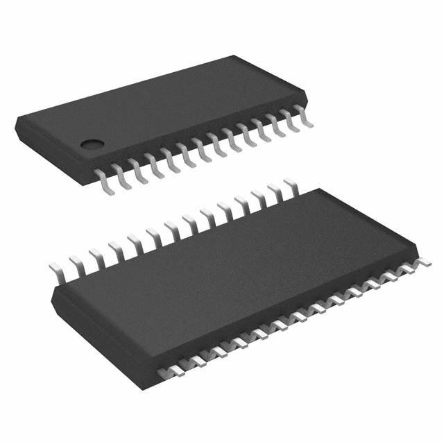
| Package | PG-TSSOP-28 (4.40 mm width) | PG-DSO-28 (7.50 mm width) | 6ED003L02F2XUMA1 is smaller and thinner, beneficial for dense layouts |
| Typical rise/fall times | 60 ns / 26 ns | 60 ns / 26 ns | Equivalent switching speed |
| Supply voltage range | 13 V to 17.5 V | 10 V to 17.5 V | 6EDL04N06PTXUMA1 supports lower supply voltages, increasing design flexibility |
Design trade-offs
The most immediate difference between these devices is the input logic polarity: the 6ED003L02F2XUMA1 features an inverting input stage, while the 6EDL04N06PTXUMA1 uses a non-inverting input. This affects the gate driver interface logic and potentially the firmware or external logic gate requirements. If your control FPGA or microcontroller directly drives these inputs, the inversion polarity must be accounted for, which can complicate the control logic or require extra inverting buffers.
From a packaging perspective, the 6ED003L02F2XUMA1 comes in a PG-TSSOP-28 package with a 4.40 mm width, compared to the larger PG-DSO-28 package (7.50 mm) of the 6EDL04N06PTXUMA1. The smaller footprint of the 6ED003L02F2XUMA1 can be a significant advantage in space-constrained designs, such as compact motor drives or embedded power modules. However, the thinner TSSOP package might have different thermal dissipation characteristics compared to the wider DSO package, potentially requiring closer attention to thermal vias and copper area in the PCB layout to maintain junction temperature limits.
Both devices support a bootstrap high-side voltage of up to 620 V, making them suitable for the same voltage class of IGBTs or MOSFETs. Their rise and fall times are identical, indicating similar switching speed performance. This means gate charge and switching losses should be comparable, assuming similar external gate resistors and MOSFETs.
The supply voltage range is slightly more flexible on the 6EDL04N06PTXUMA1, which operates from 10 V to 17.5 V, compared to 13 V to 17.5 V for the 6ED003L02F2XUMA1. This could matter if your system uses a 12 V or undervoltage-protected supply rail, as the 6ED003L04N06PTXUMA1 can function at lower voltages, potentially improving system robustness or startup behavior.
Cost data is not specified in the source data, but typically TSSOP packages (6ED003L02F2XUMA1) are lower cost and more common in volume, while DSO packages (6EDL04N06PTXUMA1) may be slightly more expensive due to size and thermal handling. However, cost differences are often marginal compared to the PCB area saved or the system architecture requirements.
Use-case fit
Choose 6ED003L02F2XUMA1 when…
- The PCB area is limited and a smaller package footprint is critical.
- Your control logic or firmware is already designed for inverting gate driver inputs.
- The supply voltage rail is fixed at or above 13 V, with no need for operation at lower voltages.
- Thermal dissipation can be managed effectively with a compact TSSOP package layout.
- The design benefits from a standardized, smaller package for 3-phase inverter gate drivers.
Choose 6EDL04N06PTXUMA1 when…
- Your control signals are non-inverted, and you want to avoid adding external inversion stages.
- The power supply rail can vary down to 10 V, requiring a gate driver that supports lower supply voltages.
- PCB space is less constrained, and the larger DSO package can be accommodated, possibly improving thermal performance.
- You want to maintain compatibility with existing designs or reference layouts that use PG-DSO-28 packages.
- The system demands slightly more robust startup behavior at lower supply voltages.
Drop-in compatibility
These parts are not pin-compatible or footprint-compatible. The 6ED003L02F2XUMA1 uses a PG-TSSOP-28 package with a narrower body and different pin spacing than the PG-DSO-28 package of the 6EDL04N06PTXUMA1. Additionally, the input logic polarity differs (inverting vs non-inverting), which means substituting one for the other requires redesigning the input signal conditioning or firmware logic. Therefore, a simple drop-in replacement is not possible without PCB and logic modifications.
Alternatives to consider
- Infineon 6EDL04N06NTXUMA1: Similar to 6EDL04N06PTXUMA1 but may have different input logic or package options worth comparing.
- Texas Instruments UCC37322: A high-speed half-bridge driver with programmable dead-time, suitable for similar voltage classes but with different control features.
- Microchip MCP1416: A dual MOSFET driver with high peak current capability, useful if separate gate drivers with flexible logic inputs are preferred.