Key Specs
| Spec | Value | Condition | Source |
|---|---|---|---|
| Mounting Type | Surface Mount | Digi-Key | |
| Operating Temperature Range | 0°C ~ 70°C (TA) | Digi-Key | |
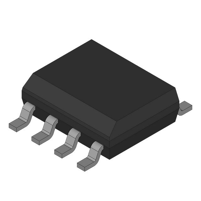
| Package Case | 8-SOIC (0.154”, 3.90mm Width) | Digi-Key | |
| Supplier Device Package | 8-SOIC | Digi-Key |
When To Use
-
Offline Flyback 12V @ 1.5A: The UC3842D8’s 8-SOIC package with a 0°C to 70°C ambient rating matches typical commercial-grade flyback designs with moderate output current. Its fixed-frequency current mode control prevents transformer saturation and limits peak current, avoiding shoot-through in the primary switch. A linear regulator here would overheat due to high power dissipation, and a synchronous buck controller would not handle isolation or input voltage spikes properly.
-
24V Battery Charger @ 3A: The UC3842D8’s current sense and oscillator circuitry support stable peak current regulation, preventing latch-up during rapid load transients common in battery charging. Its surface-mount 8-SOIC fits compact PCB layouts typical in automotive or industrial applications. Using a low-IQ PFM buck would fail to provide fast transient response and current limiting, risking battery damage.
-
Industrial 5V Isolated Power Supply @ 0.5A: The UC3842D8’s robust current mode control and switching frequency stability enable clean regulation in isolated flyback topologies with moderate output current. Its operating temperature range fits factory floor environments. A synchronous buck controller would lack isolation, causing potential ground loops and safety violations.
When Not To Use
-
High Current 12V @ 20A DC-DC Converter: The UC3842D8’s internal current sense and drive stage cannot handle currents above a few amps reliably. Use a multi-phase buck controller instead to distribute current, reduce inductor ripple, and prevent thermal runaway.
-
Battery-Powered Wearable Device: The 0°C to 70°C operating range and relatively high quiescent current make this part unsuitable for ultra-low power, long-life battery applications. Use a low-IQ PFM buck to minimize battery drain during standby.
-
Compact 3.3V @ 5A Point-of-Load Regulator Switching at >600kHz: The UC3842D8’s internal oscillator frequency range maxes well below 500kHz, limiting inductor size reduction and transient response. Use a high-frequency buck controller to achieve the needed switching speed and dynamic performance.
Application Notes
-
The switching node (SW) pin connects directly to the power MOSFET drain; minimize trace inductance here to reduce voltage overshoot and EMI. Keep the loop area between SW, current sense resistor, and ground as small as possible.
-
the Current Sense pin and the Voltage Feedback pin are highly noise sensitive; route sense signals away from high di/dt traces and use local ground returns to prevent false triggering or jitter.
-
The oscillator frequency is internally fixed but can be modulated by an external timing resistor on pin 4; ensure this resistor is stable and low noise to maintain consistent switching frequency.
-
The device’s enable pin (if used) requires a clean logic signal; any slow or noisy transitions can cause erratic switching or extended startup delay.
-
Place a high-quality ceramic bypass capacitor close to the Vcc pin and the GND pin to suppress supply noise and prevent latch-up during load transients.
Pin numbers are package-specific. Verify against the datasheet pinout diagram before routing.
Gotchas
-
[Ignoring Startup Minimum Load]: The UC3842D8 requires a minimum load on the output for stable operation; otherwise, the oscillator may fail to start or output pulses may be erratic. Symptom: no switching observed on the SW node or intermittent bursts of pulses. Fix: add a small dummy load (~few hundred mA) during startup or design for a startup bias current.
-
[Current Sense Resistor Parasitics]: Using a long PCB trace or high-inductance resistor for current sensing causes ringing and false peak detection, triggering premature cycle skipping or shutdown. Symptom: irregular switching frequency and unexplained output voltage ripple. Fix: use a low-inductance, low-ESR resistor placed as close as possible to the IC’s current sense pin, with a Kelvin connection if possible.
-
[Oscillator Frequency Shift with Temperature]: Though the specified ambient range is 0°C to 70°C, the internal oscillator frequency drifts with temperature, causing duty cycle variation if the timing resistor is not temperature compensated. Symptom: output voltage drift under temperature cycling. Fix: use a precision, low-tempco resistor for timing or implement external compensation.
-
[Ground Bounce from High dI/dt Switching Node]: Routing the SW node trace over or near the current sense and feedback ground can inject noise into the control loop, causing jitter or intermittent shutdown. Symptom: irregular PWM pulses and output voltage ripple on the scope. Fix: separate power and signal grounds with a star grounding scheme and route SW node away from sensitive pins 2 and 3.