Key Specs
| Spec | Value | Condition | Source |
|---|---|---|---|
| Battery Chemistry | Lithium Ion/Polymer | Digi-Key | |
| Number Of Cells | 1 | Digi-Key | |
| Current Charging | Constant - Programmable | Digi-Key | |
| Programmable Features | Current | Digi-Key | |
| Fault Protection | Over Temperature | Digi-Key | |
| Charge Current (Max) | 1.1A | Digi-Key | |
| Battery Pack Voltage | 4.2V | Digi-Key | |
| Voltage Supply (Max) | 6V | Digi-Key | |
| Interface | - | Digi-Key | |
| Operating Temperature Range | -40°C ~ 85°C (TA) | Digi-Key | |
| Mounting Type | Surface Mount | Digi-Key | |
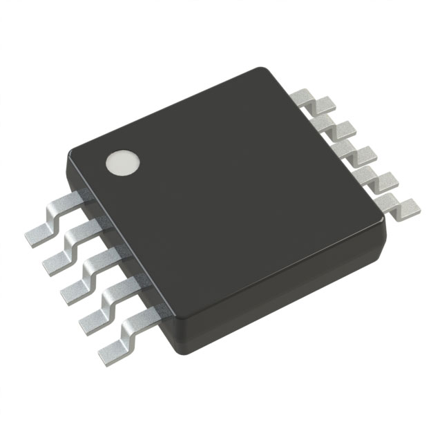
| Package Case | 10-TFSOP, 10-MSOP (0.118”, 3.00mm Width) | Digi-Key | |
| Supplier Device Package | 10-MSOP | Digi-Key |
When To Use
-
Use the MCP73833T-AMI/UN in single-cell Lithium Ion or Lithium Polymer battery charging applications where a programmable constant current charge up to 1.1 A is required (charge_current_max = 1.1 A). It is ideal for portable devices such as handheld instruments or IoT nodes that operate within an ambient temperature range of -40°C to +85°C (ambient_temperature_range).
-
The device is suitable when a surface-mount package with a small footprint is needed (package_case = 10-TFSOP, 10-MSOP, 3.00 mm width), enabling compact designs with effective thermal management.
-
Do not use this device for charging multi-cell battery packs or batteries requiring charge currents exceeding 1.1 A. For such applications, choose a charger supporting multi-cell configurations and higher current ratings.
-
Avoid using this device in environments where the operating temperature exceeds 85°C (operating_temperature_range_max), or where input voltages exceed 10 V (input_voltage_max), as this may cause device failure or thermal shutdown.
When Not To Use
-
Multi-cell battery packs (>1 cell): The MCP73833T-AMI/UN supports only a single Li-Ion/Polymer cell with preset voltage options up to 4.5V; it cannot handle series battery stacks. Use a multi-phase buck controller designed for multi-cell balancing and higher voltage regulation.
-
High output current >1.1A continuous: The maximum programmable charge current is 1.1A with internal thermal limits. For loads or charging currents exceeding this, a high-current synchronous buck with external FETs is needed to safely deliver current without thermal or current-limit faults.
-
Low quiescent current required in battery-powered standby (<100µA): With typical standby current around 100µA and max 300µA, this part is not suitable for ultra-low power applications such as coin cells or long-life IoT nodes. A low-IQ PFM buck regulator would minimize battery drain during sleep.
Application Notes
-
Place the programming resistor (PROG pin) very close to pin 5 to minimize noise pickup, as this resistor sets the charge current via a 20kΩ to 200kΩ range.
-
Use a 1µF ceramic capacitor at the input (VDD pin 1) and output (BAT pin 8) as close as possible to the device to ensure loop stability and minimize voltage transients.
-
The thermal sense (THERM pin 6) should be connected to a 10kΩ NTC thermistor placed near the battery cell; this enables overtemperature protection and prevents charging outside the safe temperature window.
-
STAT1 (pin 3) and STAT2 (pin 4) outputs require 470Ω pull-up resistors and should be routed away from switching nodes to avoid false status signaling due to EMI.
-
Minimize voltage drops on the PCB layout by using wide copper traces for high current paths (input and battery lines) and add multiple thermal vias under the device pad to improve heat dissipation and keep junction temperature within limits.
Pin numbers are package-specific. Verify against the datasheet pinout diagram before routing.
Gotchas
-
Incorrect Programming Resistor Value:
- Mistake: Using a programming resistor (Rprog) outside the specified range (e.g., significantly higher than 200 kΩ or lower than 1 kΩ).
- Failure Mode: The charge current deviates from the intended value, potentially causing undercharging or overcurrent conditions that can damage the battery or reduce battery life.
- Fix: Always select Rprog within 1 kΩ to 200 kΩ, preferably the typical 1.00 kΩ value for a 1.1 A charge current, and verify with the device’s programming equations.
-
Insufficient Input or Output Capacitance:
- Mistake: Omitting or undersizing the input bypass capacitor (less than 1 µF) or output filter capacitor (less than 4.7 µF).
- Failure Mode: Leads to unstable voltage regulation, excessive ripple, or oscillations, resulting in erratic charging behavior or device malfunction.
- Fix: Use at least 1 µF ceramic capacitor at the input and 4.7 µF ceramic capacitor at the output, placed as close as possible to the device pins.
-
**Improper Thermistor Selection or Placement: