Key Specs
| Spec | Value | Condition | Source |
|---|---|---|---|
| Battery Chemistry | Lithium Ion/Polymer | Digi-Key | |
| Number Of Cells | 1 | Digi-Key | |
| Current Charging | Constant - Programmable | Digi-Key | |
| Programmable Features | Current | Digi-Key | |
| Fault Protection | Over Voltage | Digi-Key | |
| Charge Current (Max) | 500mA | Digi-Key | |
| Battery Pack Voltage | 4.2V | Digi-Key | |
| Voltage Supply (Max) | 6V | Digi-Key | |
| Interface | - | Digi-Key | |
| Operating Temperature Range | -40°C ~ 85°C (TA) | Digi-Key | |
| Mounting Type | Surface Mount | Digi-Key | |
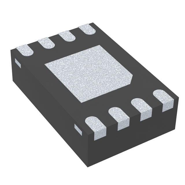
| Package Case | 8-VFDFN Exposed Pad | Digi-Key | |
| Supplier Device Package | 8-DFN (2x3) | Digi-Key |
When To Use
-
Single-cell Li-Ion battery charging @ up to 500mA: The MCP73831T-2ACI/MC is specifically designed for single-cell lithium-ion/polymer applications with a maximum charge current programmable up to 500mA. Its integrated over-voltage protection ensures safe termination without risk of battery damage, unlike a generic linear regulator which could cause thermal runaway under continuous charge at this current.
-
Battery-powered devices with low dropout voltage and 6V max supply: This device supports up to 6V input, allowing operation from USB or similar 5V sources with headroom for voltage spikes. Using a synchronous buck controller here risks latch-up or shoot-through if input voltage transients exceed the controller’s rating, whereas the MCP73831T-2ACI/MC handles these safely within its max 7V absolute limit.
-
Compact surface-mount designs requiring small 8-VFDFN with exposed pad: The 2x3mm DFN package with exposed pad supports efficient thermal dissipation for up to 500mA charge current in a minimal PCB footprint. In contrast, a multi-phase buck controller solution would require multiple external FETs and inductors, increasing board area and complexity, and risking thermal hotspots if layout is poor.
When Not To Use
-
Battery charging current demand > 500mA: The MCP73831T-2ACI/MC is limited to 500mA max charge current, so designs requiring higher currents must use a high-current synchronous buck with external FETs to supply higher load safely and efficiently.
-
Applications requiring input voltages above 6V supply max: This device’s absolute max supply voltage is 6V, which disqualifies it for higher-voltage inputs or automotive load dumps. Use a synchronous buck controller designed for higher input voltage ratings and robust transient handling.
-
Ultra-low quiescent current for coin-cell or μA sleep-mode operation: With a typical supply current of 510µA during charging and 53µA in charge complete, this part is too power-hungry for long-term standby on small batteries. A low-IQ PFM buck regulator is better suited to minimize battery drain in these scenarios.
Application Notes
-
The PROG pin (pin 3) requires a high-accuracy resistor (typically 10kΩ) to set the charge current. PCB layout should minimize stray capacitance and noise coupling on this pin to maintain stable current regulation.
-
The VSS pin (pin 1) and exposed pad must be connected to a clean, low-impedance ground plane to ensure proper thermal dissipation and reduce ground bounce that can induce erratic switching behavior.
-
The STAT pin (pin 4) outputs a charge status signal; route this trace away from noisy switching nodes to avoid false triggering or signal glitches.
-
Input supply decoupling with a low-ESR 4.7µF X7R ceramic capacitor placed close to the VDD pin is critical to suppress ripple and maintain stable UVLO thresholds around 3.45V.
-
Avoid routing any high-current paths near the PROG pin or the STAT output to minimize coupling noise and erroneous status reporting during fast charge transitions.
Pin numbers are package-specific. Verify against the datasheet pinout diagram before routing.
Gotchas
-
[PROG resistor tolerance and temperature drift ignored]: Designers often assume the PROG resistor sets a fixed current regardless of temperature. In reality, resistor tolerance plus board temperature variations can shift current by ±10% or more, causing under- or overcharging. This results in charge time deviations or battery stress. Fix: Use a precision resistor (1% or better), verify current at operating temperature, and consider temperature derating in the charge profile.
-
[Insufficient ground plane under exposed pad]: Omitting a solid thermal and electrical ground plane beneath the DFN exposed pad causes elevated junction temperatures and unstable regulation due to increased thermal resistance. Symptoms include premature thermal shutdown or erratic current regulation. Fix: Follow datasheet layout guidelines for exposed pad soldering and attach to a large copper area with multiple vias.
-
[Startup with battery voltage below preconditioning threshold]: If the battery voltage is below the preconditioning threshold (10–40%), the charger enters trickle charge mode at ~10% programmed current. Some engineers overlook that this slow charge phase can extend startup time significantly, causing a perception of “no charge.” Fix: Measure battery voltage before startup and ensure it’s above preconditioning threshold or allow sufficient startup delay.
-
[STAT pin glitching during input voltage transients]: Transient dips near the UVLO start threshold (3.45V typ) can cause the status output to toggle rapidly, confusing system logic. This is often mistaken for device malfunction. Fix: Add a small RC filter or Schmitt-trigger buffer on the STAT output line to clean up signal transitions during input voltage ramp events.