Key Specs
| Spec | Value | Condition | Source |
|---|---|---|---|
| Output Type | PWM Signal | Digi-Key | |
| Function | Step-Down | Digi-Key | |
| Output Configuration | Positive | Digi-Key | |
| Topology | Buck | Digi-Key | |
| Number Of Outputs | 1 | Digi-Key | |
| Output Phases | 2 | Digi-Key | |
| Supply Voltage (Typ) | 4.5V ~ 40V | Digi-Key | |
| Switching Frequency (Typ) | 100kHz ~ 1.6MHz | Digi-Key | |
| Duty Cycle (Max) | - | Digi-Key | |
| Synchronous Rectifier | Yes | Digi-Key | |
| Clock Sync | Yes | Digi-Key | |
| Serial Interfaces | I2C, PMBus, SMBus | Digi-Key | |
| Control Features | Enable, Frequency Control, Power Good, Soft Start, Watchdog | Digi-Key | |
| Operating Temperature Range | -40°C ~ 125°C (TA) | Digi-Key | |
| Grade | Automotive | Digi-Key | |
| Qualification | AEC-Q100 | Digi-Key | |
| Mounting Type | Surface Mount | Digi-Key | |
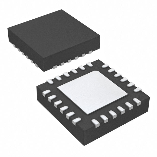
| Package Case | 24-VFQFN Exposed Pad | Digi-Key | |
| Supplier Device Package | 24-QFN (4x4) | Digi-Key |
When To Use
Use the MCP19122T-E/MJ in applications that require a highly integrated, automotive-grade, synchronous buck converter with:
- Input voltage range from 4.5V to 40V, suitable for automotive and industrial power rails.
- Switching frequencies between 100kHz and 1.6MHz, enabling compact designs with small inductors and capacitors.
- A maximum output voltage up to 16V and output current up to 2A, ideal for powering microcontrollers, sensors, and other on-board electronics.
- Integrated I2C, PMBus, and SMBus interfaces for digital control and monitoring.
- Advanced control features such as power good indication, soft start, watchdog timer, and synchronous rectification for improved efficiency.
When not to use:
- If the application requires output voltages above 16V or input voltages exceeding 40V, choose a device with higher voltage ratings.
- For applications requiring output currents above 2A continuous per phase or more than two phases, select a higher current or multi-phase controller.
- If switching frequencies below 100kHz or above 1.6MHz are needed, consider devices designed for those frequency ranges.
- For applications lacking digital interface requirements, a simpler analog controller may be more cost-effective.
When Not To Use
-
Output current > 2A continuous: The 2A max source current limits this device for higher current applications. For loads above 2A, opt for a high-current synchronous buck with external FETs to handle both current and thermal dissipation.
-
Battery-powered IoT device requiring ultra-low standby current: The 50µA shutdown quiescent current is too high for ultra-low power sleep modes. Use a low-IQ PFM buck instead to maximize battery life with sub-microamp sleep currents.
-
Switching frequency requirement above 1.6MHz: This device tops out at 1.6MHz switching frequency. For designs needing smaller inductors or tighter transient response above that, select a high-frequency buck controller capable of stable operation beyond 1.6MHz.
Application Notes
-
The PHASE pin is the switching node (SW) and must be routed with minimal loop area and wide copper to handle high di/dt currents and minimize EMI.
-
Pins GPA1 and GPB3 serve as the switching frequency synchronization signals (input or output). These pins are noise-sensitive and should be routed away from high-current loops and noisy signals to ensure stable clock sync.
-
The exposed pad (EP) must be soldered to a large thermal and ground plane connected to the P pin (large-signal power ground) to optimize thermal dissipation and minimize ground impedance.
-
Bootstrap capacitor connected to BOOT pin should be placed as close as possible to the IC pins (BOOT to PHASE) with low-ESR ceramic capacitor to maintain stable high-side driver voltage.
-
Voltage sense pins (+V and -V) for the differential amplifier require careful routing and star grounding to avoid noise coupling and ensure accurate output voltage regulation and fault detection.
Minimum External Components
Input capacitor — ≥100µF electrolytic + 100nF ceramic (parallel) Selection: Electrolytic handles bulk ripple current; ceramic bypasses switching spikes. Voltage rating ≥ 40V with 20% margin. Failure mode: Insufficient input capacitance: supply rail collapses during switch-on current demand → output droops → erratic regulation and potential latch-up.
Output capacitor — ≥100µF electrolytic Selection: ESR < 200mΩ to keep output ripple below 50mVpp. Voltage rating ≥ 20V. Failure mode: High-ESR electrolytic: output ripple voltage = ESR × ΔIL. At 1A ripple and 500mΩ ESR → 500mVpp ripple — exceeds spec for virtually all loads.
Gotchas
-
Incorrect Inductor Selection:
- Mistake: Using an inductor with insufficient current rating or too low inductance.
- Failure Mode: Inductor saturates under load, causing excessive ripple current, increased losses, and potential device shutdown due to overcurrent detection.
- Fix: Select an inductor rated for at least 2A with inductance suitable to maintain continuous conduction mode at the chosen switching frequency (100kHz to 1.6MHz). Verify inductor saturation current and DCR.
-
Bootstrap Capacitor Omission or Undersizing:
- Mistake: Omitting the bootstrap