Key Specs
| Spec | Value | Condition | Source |
|---|---|---|---|
| Amplifier Type | Current Sense | Digi-Key | |
| Gain Bandwidth Product | 125 kHz | Digi-Key | |
| Mounting Type | Surface Mount | Digi-Key | |
| Number Of Circuits | 1 | Digi-Key | |
| Operating Temperature Range | -40°C ~ 85°C | Digi-Key | |
| Output Type | - | Digi-Key | |
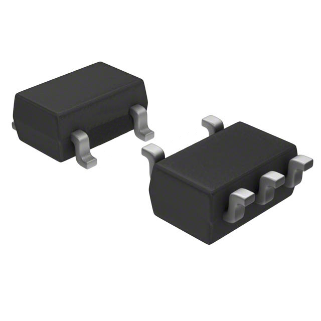
| Package Case | SC-74A, SOT-753 | Digi-Key | |
| Quiescent Current (Typ) | 1.1µA | Digi-Key | |
| Slew Rate | - | Digi-Key | |
| Supplier Device Package | SOT-23-5 | Digi-Key | |
| Voltage Input Offset | 100 µV | Digi-Key |
When To Use
-
Low-current battery monitoring → 5A @ 3.3V: The 1.1µA quiescent current makes this part the right fit for ultra-low-power battery-powered systems. A higher-quiescent-current current-sense amplifier would drain the battery faster, causing premature shutdown or reduced runtime.
-
Precision shunt measurement in space-constrained sensor nodes → 1A @ 3.3V: The SOT-23-5 package minimizes PCB area, enabling tight layouts in compact sensor modules. Larger packages would increase board size and complicate thermal management due to higher thermal resistance.
-
Industrial current sensing with tight offset requirements → 2A @ 12V: The 100µV input offset voltage supports accurate low-level current measurements without significant error. A higher-offset amplifier would introduce measurement drift, potentially causing false overcurrent triggers or poor system calibration.
When Not To Use
-
Fast transient current monitoring in motor drives: The 125 kHz gain-bandwidth product is too low for high-frequency current ripple measurement. Use a higher-bandwidth current-sense amplifier to avoid aliasing and inaccurate current waveform capture.
-
Measuring current on isolated high-voltage rails: The MAX9634FEUK+T has no galvanic isolation and must be referenced to the same ground as the shunt resistor. Use an isolated current-sense amplifier to prevent ground loops and ensure operator safety.
-
Current telemetry with digital readout and accumulation: This part outputs an analog voltage only, with no built-in digital interface or counters. Use an integrated digital current/power monitor with I²C/SMBus interface where system-level monitoring and logging is required.
Application Notes
-
The SOT-23-5 package limits PCB footprint but increases thermal resistance; place the device close to the shunt resistor with a short, low-inductance copper path to maintain accuracy and stable temperature.
-
Pins 1 and the input terminals pin are noise-sensitive; route these traces away from switching nodes or high-current traces to minimize input offset errors caused by EMI coupling.
-
Guard ring routing around the input pins is recommended to reduce leakage currents on high-humidity or contaminated PCBs; this helps maintain the 100µV offset integrity over time.
-
Avoid placing the MAX9634FEUK+T near hot components or in thermal hotspots because the small SOT-23-5 package has poor heat dissipation, which can shift offset voltage and degrade accuracy.
-
The output pin should drive high-impedance loads only; excessive loading can distort the output voltage and reduce measurement fidelity.
Related Calculators
- Current Sense / Shunt Resistor Calculator — Size your shunt resistor for this amplifier
Gotchas
-
[Ignoring input bias current effects on offset]: Designers may assume the 100µV input offset voltage dominates error, ignoring that input bias currents through high-value shunt resistors generate additional voltage errors. Result: unexpected offset drift seen on scope, inconsistent with datasheet offset specs. Fix: use lower-value shunt resistor or verify input bias current impact with bench measurements.
-
[Failing to de-rate input common-mode voltage]: The datasheet specifies an absolute maximum input voltage relative to supply rails (not in verified specs here; verify with datasheet). Applying voltages near or beyond this limit causes latch-up or device failure, even if output appears normal at first. Fix: confirm operating input voltages are within absolute max ratings with margin.
-
[Routing input traces over noisy switching nodes]: The SOT-23-5 package pins 1 and 2 are close together; routing one input trace near a high-current switching node (SW) causes capacitive coupling. Result: noisy output waveform and measurement jitter. Fix: separate sensitive input traces physically and use ground shields between them.
-
[Assuming easy rework]: The small SOT-23-5 package makes manual soldering and rework difficult; excessive heat during reflow or hot air can cause package warping or lifted pads, leading to intermittent connections. Fix: use controlled soldering profiles and inspection tools; consider automated assembly for consistency.