LM2596T-ADJ/NOPB vs. LNK3206D-TL: A Practical Comparison
Quick verdict: For simple, low-cost, through-hole buck converters where isolation isn’t needed and component count needs to be minimized, the LM2596T-ADJ/NOPB is the clear winner. However, if you need a flexible topology (buck, buck-boost, flyback) with integrated protection and are comfortable with surface-mount, the LNK3206D-TL offers significant advantages, particularly in designs requiring higher efficiency or more complex control schemes.
Spec Comparison Table
| Spec | LM2596T-ADJ/NOPB | LNK3206D-TL | Notes |
|---|---|---|---|
| Function | Step-Down | Buck, Buck-Boost, Flyback | LNK3206D-TL offers significantly more topology flexibility. |
| Output Configuration | Positive | Non-Isolated | LNK3206D-TL is non-isolated, which impacts safety and EMC design. |
| Topology | Buck | Buck, Buck-Boost, Flyback | As above. |
| Output Type | Adjustable | - | LM2596T-ADJ/NOPB’s adjustability is a benefit for fine-tuning output voltage. |
| Number of Outputs | 1 | - | Both are single-output devices. |
| Input Voltage Min | 4.5V | - | LM2596T-ADJ/NOPB’s lower minimum input voltage can be advantageous in some applications. |
| Input Voltage Max | 40V | - | LM2596T-ADJ/NOPB’s maximum input voltage is higher, providing greater design margin. |
| Output Voltage Min | 1.2V | - | LM2596T-ADJ/NOPB’s lower minimum output voltage is beneficial for some designs. |
| Output Voltage Max | 37V | - | LM2596T-ADJ/NOPB’s higher maximum output voltage is advantageous for higher-voltage applications. |
| Output Current Max | 3A | - | Both are rated for similar maximum output current. |
| Switching Frequency Typ | 150kHz | 66kHz | The LM2596’s higher frequency generally allows for smaller external components, but can also increase switching losses. |
| Synchronous Rectifier | No | No | Neither part includes synchronous rectification, which limits efficiency, especially at lower output voltages. |
| Operating Temperature Range (TJ) | -40°C ~ 125°C | -40°C ~ 125°C | Identical operating temperature range. |
| Mounting Type | Through Hole | Surface Mount | LM2596’s through-hole nature simplifies prototyping but complicates automated assembly. |
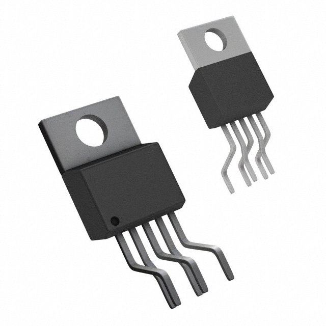
| Package Case | TO-220-5 Formed Leads | 8-SOIC (0.154”, 3.90mm Width), 7 Leads | The TO-220 package is larger and easier to handle, while the SOIC is more compact for dense designs. |
| Supplier Device Package | TO-220-5 | SO-8C | As above. |
| Internal Switch | No | Yes | The LNK3206D-TL’s integrated switch simplifies the design and reduces BOM cost. |
| Voltage Breakdown | - | 725V | LNK3206D-TL’s higher breakdown voltage provides greater safety margin. |
| Duty Cycle | - | 69% | LNK3206D-TL’s duty cycle limitation impacts design flexibility. |
| Fault Protection | - | Current Limiting, Over Temperature, Over Voltage, Short Circuit | LNK3206D-TL’s integrated protection reduces BOM cost and simplifies design. |
Design Trade-offs
The most significant difference lies in the integrated nature of the LNK3206D-TL. The LM2596T-ADJ/NOPB requires external components for virtually everything – switching MOSFET, diode, inductor, and external compensation. This gives you more design freedom to optimize individual components, but also increases BOM cost, PCB area, and design complexity. The LNK3206D-TL integrates a switch, simplifying the BOM and reducing PCB area. However, this also means less control over individual component selection and a fixed duty cycle limitation.
Efficiency curves are difficult to compare directly without detailed application-specific testing. However, the LNK3206D-TL’s integrated switch and potentially more advanced control schemes could offer higher efficiency in some applications, particularly at higher loads. The LM2596’s 150kHz switching frequency, while allowing for smaller components, also increases switching losses.
Thermal considerations are important for both parts. The LM2596, with its external MOSFET and diode, can be easier to thermally manage due to the ability to use larger components and heatsinks. The LNK3206D-TL, being a smaller surface-mount package, requires careful PCB layout to dissipate heat effectively.
Gate drive is a non-issue with the LM2596, as it’s a complete IC. The LNK3206D-TL’s internal gate drive is handled internally, simplifying the design.
Layout sensitivity is higher for the LM2596 due to the need for careful routing of high-current loops and external compensation network design. The LNK3206D-TL’s smaller size and integrated components reduce layout complexity, but still require careful attention to ground plane integrity.
Cost at volume is difficult to definitively state without quotes, but the LNK3206D-TL’s reduced BOM count and smaller PCB area could lead to lower overall system cost, despite potentially higher unit cost.
Use-case Fit
Choose LM2596T-ADJ/NOPB when…
- You need a simple, low-cost buck converter for prototyping or low-volume production.
- Through-hole mounting is preferred for ease of assembly or repair.
- You require maximum design flexibility to optimize individual components.
- You’re working with a higher input voltage, up to 40V.
- You need an adjustable output voltage with a wide range, from 1.2V to 37V.
- You are building a power supply for a legacy device that requires a simple, robust design.
Choose LNK3206D-TL when…
- You need a compact solution with a smaller PCB footprint.
- You require a flexible topology (buck, buck-boost, flyback) for a more complex application.
- You want to reduce BOM cost and simplify design by leveraging an integrated solution.
- You need integrated protection features to improve reliability and reduce design effort.
- You are designing a power supply for a battery-powered device where efficiency and size are critical.
- You need to implement a buck-boost topology to handle varying input voltage conditions.
Drop-in Compatibility
These parts are not pin-compatible or footprint-compatible. The LM2596T-ADJ/NOPB uses a TO-220 package with five leads, while the LNK3206D-TL uses an 8-SOIC package. Substituting one for the other would require a complete PCB redesign, including changes to the power stage, control circuitry, and feedback network.
Alternatives to Consider
- LM2596S-ADJ: A lower-cost alternative to the LM2596T-ADJ, suitable for less demanding applications.
- Texas Instruments TPS5430: A synchronous buck converter offering higher efficiency and more advanced features.
- Power Integrations LNK4094: A similar integrated controller offering a different set of features and performance characteristics.