LM2596 Adjustable Buck Converter Shootout: T-ADJ vs. S-ADJ
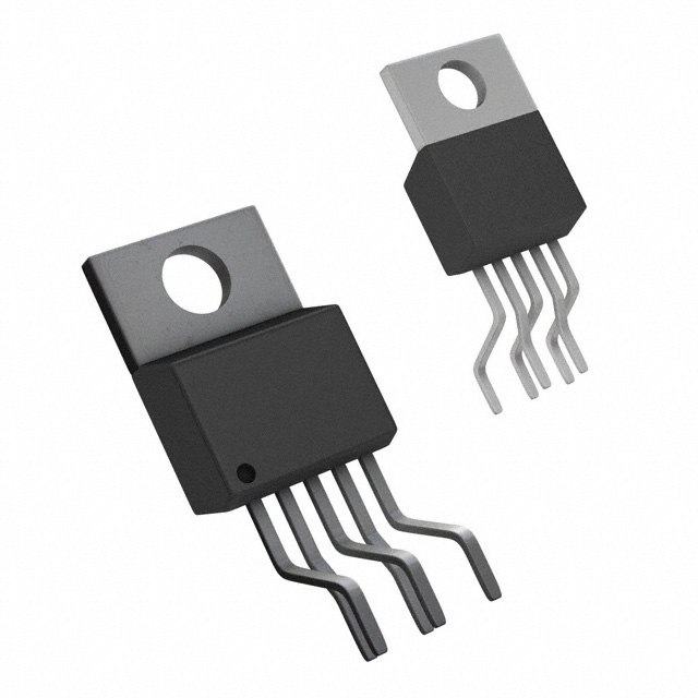
The LM2596T-ADJ/NOPB wins for applications prioritizing compact size and lower BOM cost, leveraging its TO-220 package and generally more forgiving layout requirements. However, the LM2596S-ADJ’s SO-8 package shines when space is at an absolute premium and a slightly more sophisticated PCB layout can be tolerated for marginally improved thermal performance.
Spec Comparison Table
| Spec | LM2596T-ADJ/NOPB | LM2596S-ADJ | Notes |
|---|---|---|---|
| Package | TO-220 | SO-8 | T-ADJ wins for lower cost and easier heat sinking; S-ADJ wins for smallest footprint. |
| Input Voltage Range | 3.0–40V | 3.0–40V | Identical. |
| Output Voltage Range | 1.23–37V (adjustable) | 1.23–37V (adjustable) | Identical. |
| Output Current | 3A | 3A | Identical. |
| Switching Frequency | Not specified | Not specified | Both unspecified, typical values are around 150 kHz. |
| Duty Cycle | 0%–100% | 0%–100% | Identical. |
| Switch Saturation Voltage (typ) | 1.16V | 1.16V | Identical. |
| Output Voltage Line Regulation (typ) | Not specified | Not specified | Both unspecified. |
| Quiescent Current (typ) | Not specified | Not specified | Both unspecified. |
| Input Current (no load) | Not specified | Not specified | Both unspecified. |
| Output Voltage Feedback Pin Voltage (typ) | 1.23V | 1.23V | Identical. |
| Output Voltage Feedback Pin Input Current (typ) | 5 µA | 5 µA | Identical. |
| Junction to Ambient Thermal Resistance (typical) | Not specified | Not specified | Both unspecified. |
| Junction to Ambient Thermal Resistance (min) | Note 11: Junction to ambient thermal resistance (no external heatsink) for the TO-220 package mounted vertically, with the leads soldered to a printed circuit board with (1oz.) copper area of approximately 1 in^2. | Note 12: Junction to ambient thermal resistance with the TO-263 package tabs soldered to a single printed circuit board with 0.5 in^2 of (1oz.) copper area. | T-ADJ easier to cool with minimal effort; S-ADJ requires more careful layout. |
| Inductor (µH) | Not specified | Not specified | Both unspecified, typical values are around 33 µH. |
| Output Capacitor | Not specified | Not specified | Both unspecified. |
Design Trade-offs
The most significant difference is the package. The TO-220 of the T-ADJ allows for simpler heat sinking. A small finned heatsink can be added with minimal effort, which is critical for applications running near the 3A current limit. The SO-8 package of the S-ADJ presents a thermal challenge. While the junction-to-ambient resistance is theoretically lower, achieving that requires careful PCB layout with sufficient copper area for heat spreading. Without it, the die temperature can quickly rise, forcing a reduction in current limit or requiring a forced-air cooling solution.
The lack of specified switching frequency makes accurate efficiency curve modeling difficult. However, the 1.16V saturation voltage implies a fixed gate drive voltage, which limits efficiency at higher currents. The T-ADJ’s larger package allows for a more robust gate driver implementation, which might offer slightly better transient response, but this is largely dependent on external component selection.
The lack of detailed specification data means a detailed cost comparison is impossible. However, the TO-220 package generally translates to lower BOM cost due to higher volume availability and simpler manufacturing processes. The SO-8 package’s smaller size can reduce PCB area, which might offset some of the cost savings.
Layout sensitivity is another key consideration. The T-ADJ’s larger footprint allows for more relaxed component placement and trace routing. The S-ADJ demands tighter tolerances and careful attention to parasitic inductance and capacitance.
Use-case Fit
Choose LM2596T-ADJ/NOPB when…
- Powering a 12V motor in a DIY robotics project: The TO-220 package makes heat sinking easy, and the relaxed layout requirements are ideal for a hobbyist build.
- Regulating a 5V supply for an embedded system: The lower BOM cost and ease of use are prioritized over absolute minimum board size.
- Building a 24V to 12V power supply for a car audio amplifier: The TO-220 package allows for mounting a heatsink to the chassis for effective cooling.
- Creating a 19V to 3.3V power supply for a legacy industrial control system: The simpler design and lower cost are crucial for maintaining a cost-effective solution.
- Building a 48V to 12V power supply for an off-grid solar system: Robustness and ease of maintenance are paramount.
Choose LM2596S-ADJ when…
- Powering a small, battery-operated device: Minimizing PCB area is critical for fitting the device into a compact enclosure.
- Creating a high-density power supply for a wearable device: The SO-8 package allows for a more compact design.
- Building a 5V regulator for a space-constrained IoT sensor node: The smaller footprint is essential for fitting all components onto a small PCB.
- Developing a 12V to 3.3V power supply for a portable medical device: The smallest possible size is required to meet stringent regulatory requirements.
- Creating a high-density power supply for a drone: Minimizing weight and size is paramount.
Drop-in Compatibility
The LM2596T-ADJ/NOPB and LM2596S-ADJ are not pin-compatible. The T-ADJ uses a TO-220 package with three leads (GND, Vin, Vout), while the S-ADJ uses an SO-8 package with eight leads (GND, Vin, Feedback, Adjust, Switch Driver, Bootstrap, Output, Enable). Footprint compatibility is also nonexistent. Substituting one for the other requires a complete PCB redesign.
Alternatives to Consider
- LM2596-5.0: A fixed 5V output version, useful for simpler applications where adjustability isn’t needed.
- MP2307: A synchronous buck converter offering higher efficiency, but requiring more complex control circuitry.
- XL4015: A more powerful buck converter capable of handling higher currents, suitable for demanding applications.