Key Specs
| Spec | Value | Condition | Source |
|---|---|---|---|
| Control Features | - | Digi-Key | |
| Duty Cycle | - | Digi-Key | |
| Fault Protection | Current Limiting, Over Temperature, Over Voltage | Digi-Key | |
| Internal Switch S | Yes | Digi-Key | |
| Mounting Type | Surface Mount | Digi-Key | |
| Operating Temperature Range | -40°C ~ 105°C (TA) | Digi-Key | |
| Output Isolation | Isolated | Digi-Key | |
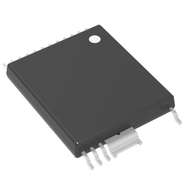
| Package Case | 24-PowerSMD Module (0.425”, 10.80mm Width), 17 Leads | Digi-Key | |
| Power Watts | 75 W | Digi-Key | |
| Supplier Device Package | InSOP-24D | Digi-Key | |
| Supply Voltage (Typ) | - | Digi-Key | |
| Switching Frequency (Typ) | 70kHz | Digi-Key | |
| Topology | Flyback, Secondary Side SR | Digi-Key | |
| Voltage Breakdown | 750V | Digi-Key |
When To Use
-
48V input → 12V @ 6A isolated output: The 750V breakdown and isolated secondary side synchronous rectification suit this flyback topology perfectly, supporting up to 75W power with built-in internal switches. Using a non-isolated synchronous buck controller here risks damaging downstream circuitry due to lack of galvanic isolation and exposes the system to ground loop noise and safety violations.
-
Industrial sensor power module @ 24V out, 3A: The integrated synchronous rectifier on the secondary side and 70kHz switching frequency optimize efficiency within the 75W power envelope, reducing thermal stress in a compact InSOP-24D package. A standard flyback with diode rectification would increase losses, potentially causing thermal runaway under continuous heavy load.
-
Battery charger providing isolated 5V @ 10A max: The 24-lead InSOP package and current limiting fault protection ensure reliable operation near the 75W limit with thermal and overvoltage safeguards. A simple LDO or linear approach would dissipate excessive heat, while a non-isolated flyback controller cannot provide the required galvanic isolation and would cause latch-up or damage downstream.
When Not To Use
-
High-current server VRM delivering >20A: The 75W power rating and internal switches limit output current and power density. Use a multi-phase buck controller designed for high current and load sharing instead.
-
Battery-powered sensor with μA sleep current: The internal switch and fixed 70kHz switching frequency imply higher quiescent current unsuitable for long battery life. Use a low-IQ PFM buck to minimize quiescent current in standby.
-
High-frequency switching >500kHz for small magnetics: The fixed 70kHz switching frequency cannot support designs requiring very small inductors or transformers. Use a high-frequency buck controller to achieve switching above 500kHz.
Application Notes
-
The SW node (pin 8) switches at 70kHz with high dv/dt; route its traces short and wide to minimize EMI and voltage overshoot. Keep sensitive feedback pins (pins 3 and 5) physically distant from SW to reduce noise coupling.
-
Pins 13 and 14 handle synchronous rectification drive signals; ensure tight coupling with secondary-side transformer windings and minimize loop area to prevent erratic SR operation.
-
Guard routing is recommended around the thermal pad and power pins (pins 1, 2, 16) to improve heat dissipation and reduce ground bounce, especially under high load conditions.
-
The internal current limiting and overvoltage protection circuits rely on accurate input voltage sensing; place input decoupling capacitors (ceramic and bulk) as close as possible to the supply pins (pins 17 and 24).
-
External BOM capacitance on the output must maintain ESR within recommended limits to avoid instability; low-ESR ceramic caps in parallel with tantalum or electrolytic capacitors are advised.
Pin numbers are package-specific. Verify against the datasheet pinout diagram before routing.
Gotchas
-
[Startup sequencing on isolated flyback]: Assuming the device will start correctly without applying the proper bias to the auxiliary winding on primary side or missing minimum load on the secondary can cause the IC to stall in undervoltage lockout. Symptom: output never reaches regulation and switching is intermittent or absent. Fix: design a minimum load or pre-bias circuit and verify auxiliary winding startup voltage during bench testing.
-
[Ignoring ESR requirements on output capacitors]: Designers may choose all-ceramic low-ESR capacitors assuming better ripple performance. However, too low ESR can destabilize the secondary side synchronous rectifier control loop, causing output voltage oscillations visible on scope as ringing or periodic overshoot. Fix: include a small ESR component by paralleling a tantalum or special polymer capacitor and verify loop stability with a bode plot.
-
[Unshielded SW node routing]: Routing the SW node over or near sensitive control pins (e.g., feedback or enable) without guard traces or ground shielding leads to high-frequency noise coupling, triggering false fault shutdowns (overvoltage or current limit). Symptom: intermittent shutdowns or erratic switching frequency jitter. Fix: isolate SW traces with ground guard rings and maintain at least 3mm separation from sensitive pins.
-
[Thermal derating at high ambient]: The specified 105°C max operating ambient assumes proper PCB thermal management and airflow. Overlooking the InSOP-24D package’s footprint and copper area leads to unexpected thermal derating, causing the internal switches to enter thermal shutdown under full load. Fix: perform thermal imaging during prototype testing and increase copper area or add forced convection as needed.