Key Specs
| Spec | Value | Condition | Source |
|---|---|---|---|
| Current Continuous Drain ID 25 C | 97A (Tc) | Digi-Key | |
| Drain-source Voltage (Max) | 1200 V | Digi-Key | |
| Drive Voltage Max RDS On Min RDS On | 15V, 18V | Digi-Key | |
| FET Feature | - | Digi-Key | |
| FET Type | N-Channel | Digi-Key | |
| Gate Charge Qg Max VGS | 89 nC @ 18 V | Digi-Key | |
| Gate-source Voltage (Max) | +23V, -7V | Digi-Key | |
| Grade | - | Digi-Key | |
| Input Capacitance Ciss Max VDS | 2910 pF @ 800 V | Digi-Key | |
| Mounting Type | Through Hole | Digi-Key | |
| Operating Temperature Range | -55°C ~ 175°C (TJ) | Digi-Key | |
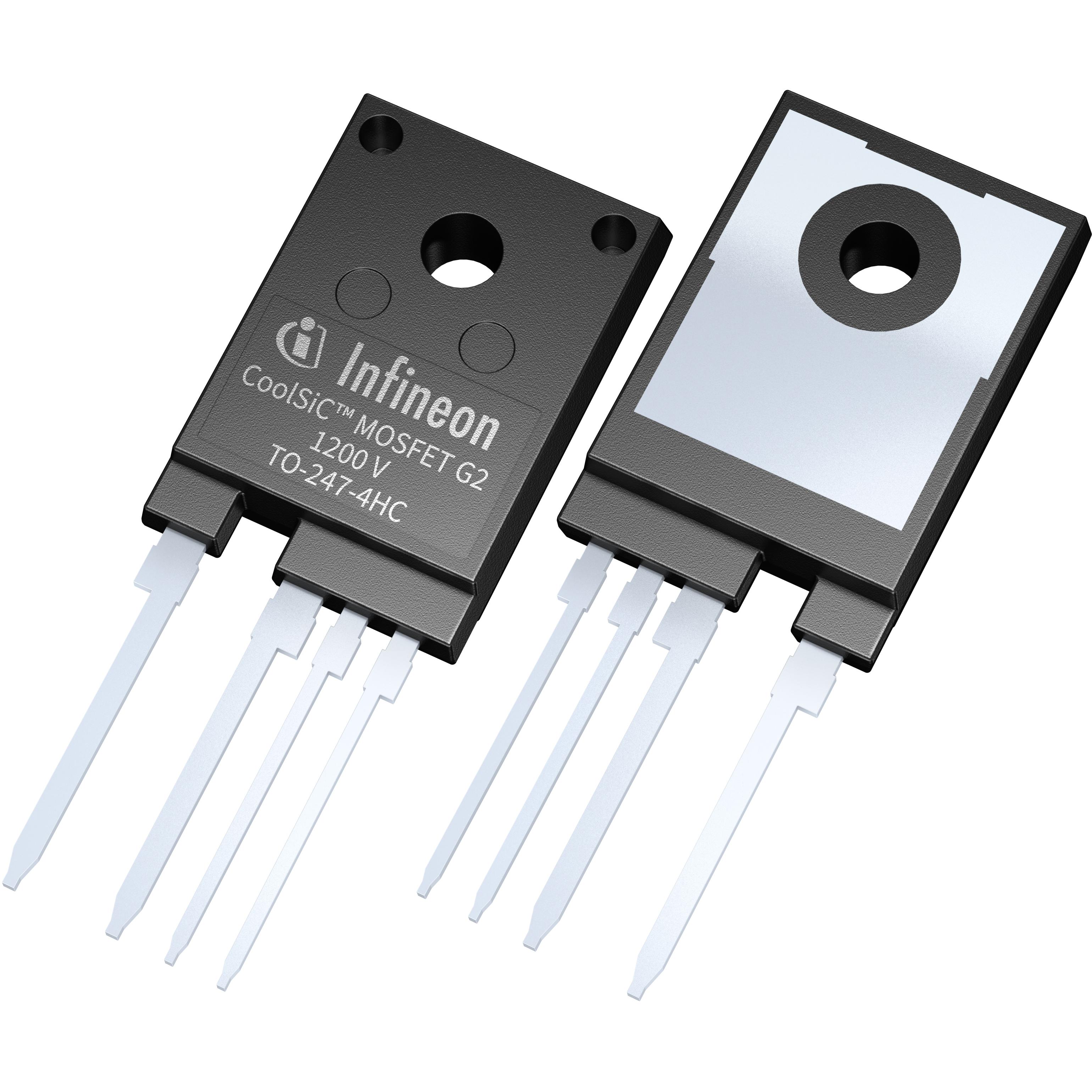
| Package Case | TO-247-4 | Digi-Key | |
| Power Dissipation (Max) | 382W (Tc) | Digi-Key | |
| Qualification | - | Digi-Key | |
| RDS On Max ID VGS | 17mOhm @ 40A, 18V | Digi-Key | |
| Supplier Device Package | PG-TO247-4-17 | Digi-Key | |
| Technology | SiCFET (Silicon Carbide) | Digi-Key | |
| VGS Th Max ID | 5.1V @ 12.7mA | Digi-Key |
When To Use
Use the IMZC120R017M2HXKSA1 in high-voltage, high-current applications requiring robust SiC MOSFET performance, such as industrial motor drives or power supplies, where a maximum drain-source voltage of 1200 V and continuous drain current of 97 A (at Tc) are required. Its low Rds(on) of 17 mΩ at 40 A and 18 V gate drive makes it well-suited for efficient power conversion with minimized conduction losses.
Do not use this device in low-voltage (< 600 V) or low-current applications where smaller, lower-cost MOSFETs with lower gate charge might be more appropriate. For such cases, consider alternative MOSFETs optimized for lower voltage and lower current ratings.
When Not To Use
-
Output Current > 100 A Continuous: The 97 A continuous current limit disqualifies this MOSFET for very high current loads. Use a multi-phase buck controller solution with parallel FETs to share current and reduce thermal stress.
-
Switching Frequency > 500 kHz Needed: The gate charge and gate drive requirements make this device inefficient and prone to excessive switching losses at very high frequencies. Opt for a high-frequency buck controller designed for low gate charge and fast switching.
-
Input-Output Voltage Differential < 1 V with Noise Sensitivity: The relatively high gate threshold (5.1 V max) and switching node noise make this unsuitable for low dropout linear regulation or precision applications. Use an LDO regulator for clean, low-noise low-voltage regulation.
Application Notes
The drain terminal switches at high voltage and high current, so the switching node loop area must be minimized to reduce parasitic inductances and voltage overshoot. The gate pin is noise-sensitive; use proper gate drive layout techniques and shielding to prevent false triggering. Given the maximum power dissipation of 382 W at Tc, a suitable heatsink is required under continuous high-current operation to maintain junction temperature within the specified -55°C to 175°C range.
Gotchas
-
Applying gate-source voltage beyond the maximum rating of +23 V or below -7 V can permanently damage the gate oxide, leading to device failure. Always ensure gate drive circuits are designed to stay within these limits.
-
Inadequate thermal management can cause the junction temperature to exceed the maximum operating range of -55°C to 175°C (TJ), resulting in device degradation or failure. Use appropriate heatsinking and ensure the device operates within the 382 W maximum power dissipation at Tc.