Key Specs
| Spec | Value | Condition | Source |
|---|---|---|---|
| Control Features | Soft Start | Digi-Key | |
| Duty Cycle | 72% | Digi-Key | |
| Fault Protection | Current Limiting, Open Loop, Over Load, Over Temperature, Over Voltage | Digi-Key | |
| Internal Switch S | Yes | Digi-Key | |
| Mounting Type | Through Hole | Digi-Key | |
| Operating Temperature Range | -40°C ~ 150°C (TJ) | Digi-Key | |
| Output Isolation | Isolated | Digi-Key | |
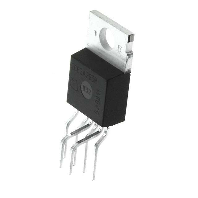
| Package Case | TO-220-6 Formed Leads | Digi-Key | |
| Power Watts | 111 W | Digi-Key | |
| Supplier Device Package | PG-TO220-6-47 | Digi-Key | |
| Supply Voltage (Typ) | 8.5V ~ 21V | Digi-Key | |
| Switching Frequency (Typ) | 100kHz | Digi-Key | |
| Topology | Flyback | Digi-Key | |
| Voltage Breakdown | 800V | Digi-Key | |
| Voltage Start Up | 13.5 V | Digi-Key |
When To Use
Use the ICE2A380P2BKSA1 in isolated flyback power supply designs requiring up to 111 W power output and an 800 V voltage breakdown rating. Its 100 kHz switching frequency and through-hole PG-TO220-6 package make it suitable for industrial and consumer applications where robust fault protection (current limiting, open loop, overload, over temperature, over voltage) and wide operating temperature range (-40°C to 150°C) are critical. Avoid using this device in non-isolated topologies or applications demanding switching frequencies significantly higher than 100 kHz; in such cases, consider a device optimized for higher frequency operation and alternative topologies.
When Not To Use
-
>10A output current rail: The maximum output power rating of 111 W and integrated MOSFET limit continuous current capability. Use a high-current synchronous buck with external FETs to handle higher currents with efficient thermal management.
-
Battery-powered sensor needing μA sleep currents: The internal switch and continuous 100 kHz switching frequency imply relatively high quiescent current. Use a low-IQ PFM buck controller designed for ultra-low standby consumption.
-
High-frequency resonant converter at 1MHz switching: The fixed 100 kHz switching frequency and flyback topology prevent operation at frequencies >500 kHz. Use a high-frequency buck controller to meet inductor size and EMI requirements.
Application Notes
The internal switch pin switches at the primary side and requires the smallest possible loop area to reduce switching losses and EMI. The feedback/control pin is noise-sensitive and should be routed away from high-current switching nodes. Given the device’s 111 W power rating and maximum junction temperature of 150°C, a suitable heatsink is necessary under typical operating conditions to ensure reliable thermal performance.
Gotchas
-
Mistake: Designing the PCB with a large switching node loop area.
Failure Mode: Increased EMI and potential instability due to high switching noise.
Fix: Minimize the loop area around the internal switch node by placing the device and associated components close together and using tight, low-inductance layouts. -
Mistake: Operating the device without adequate thermal management at high load conditions.
Failure Mode: Device junction temperature exceeding 150°C, leading to thermal shutdown or permanent damage.
Fix: Use an appropriate heatsink on the TO-220-6 package to maintain junction temperature within the specified range during continuous operation at or near the 111 W power rating.