Key Specs
| Spec | Value | Condition | Source |
|---|---|---|---|
| Current Startup | 30 µA | Digi-Key | |
| Mode | Continuous Conduction (CCM) | Digi-Key | |
| Mounting Type | Surface Mount | Digi-Key | |
| Operating Temperature Range | -40°C ~ 105°C | Digi-Key | |
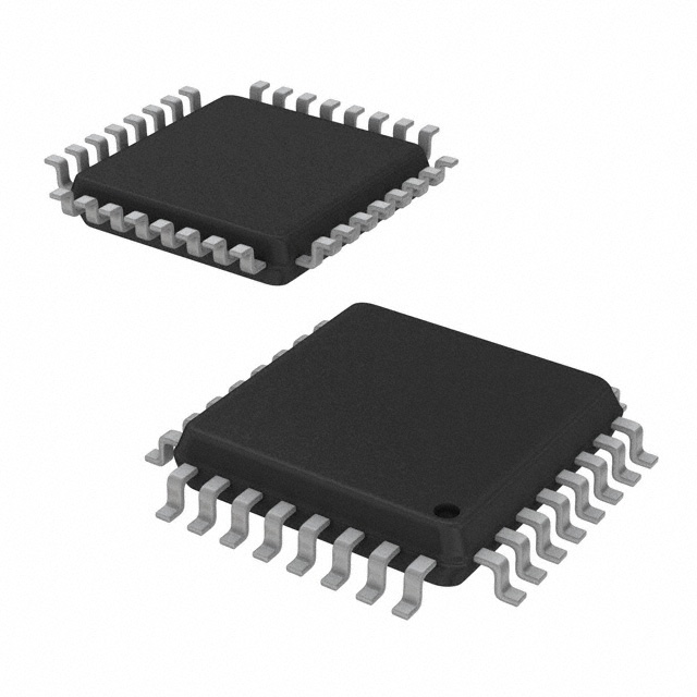
| Package Case | 32-LQFP | Digi-Key | |
| Supplier Device Package | 32-LQFP (7x7) | Digi-Key | |
| Switching Frequency (Typ) | 18kHz ~ 40kHz, 55kHz ~ 75kHz | Digi-Key | |
| Voltage Supply | 15V | Digi-Key |
When To Use
-
15V input → 5V @ 1A: The 15V supply voltage rating and 32-LQFP package support moderate power levels with good thermal dissipation. Using a linear regulator here would cause excessive heat dissipation (≈10W) and immediate thermal shutdown, making this switching controller the right choice.
-
Battery-powered motor driver, 18kHz switching: The low startup current of 30 µA combined with a low switching frequency range starting at 18kHz minimizes switching losses and quiescent current, extending battery life. A high-frequency buck controller would waste power in switching losses, causing premature battery drain.
-
Industrial control board with surface mount: The 32-LQFP (7x7 mm) package and -40°C to 105°C operating range make this part ideal for industrial environments with wide temperature swings and tight PCB real estate. Discrete synchronous buck solutions or multi-phase controllers may fail due to larger size or insufficient temperature margins.
When Not To Use
-
>10A output current: The FAN9673Q’s internal design and package limit peak current capability. For output currents exceeding this rating, use a high-current synchronous buck with external FETs to handle higher currents safely and efficiently.
-
Light-load IoT node in sleep mode: The 30 µA startup current is too high for battery-powered applications where quiescent current dominates. Use a low-IQ PFM buck controller optimized for ultra-low standby consumption.
-
Compact, noise-sensitive RF front-end with <1V dropout: The FAN9673Q’s switching frequency range and topology do not optimize low noise or low dropout. Use an LDO regulator for minimal output ripple and tight voltage regulation.
Application Notes
-
The switching node (SW) pin must have minimal loop area with input and output capacitors to reduce EMI and ringing; keep this loop physically small and place ceramic capacitors as close as possible.
-
Pins 5 and 12 are noise-sensitive feedback and compensation nodes; route these away from noisy digital traces and switching nodes to maintain stability and prevent jitter.
-
The ground return for the power stage and control stage should be separated and joined at a single point near the IC’s thermal pad to reduce ground bounce.
-
Use guard traces or ground fills around the feedback and compensation pins to shield from radiated noise, especially when switching at the higher 55kHz–75kHz frequency window.
-
Ensure input supply voltage does not exceed 15 V under transient conditions; use a transient voltage suppressor or clamp if necessary to protect the IC.
Gotchas
-
Startup under light load: Assuming the FAN9673Q will start smoothly into no-load or very light-load conditions can fail. The internal current sensing and mode control require a minimum load to avoid oscillation or output voltage undershoot. Symptom: output voltage ripple or hiccups at startup seen on scope. Fix: add a small bleed resistor or minimum load to stabilize startup.
-
Switching frequency band jump: The device switches between 18kHz–40kHz and 55kHz–75kHz ranges depending on operating conditions or external resistor settings. If layout or compensation components are optimized only for the lower band, unexpected instability or excessive EMI can appear when the controller switches to the higher band. Fix: validate compensation and EMI suppression at both frequency ranges.
-
Thermal pad soldering and mounting: Insufficient solder under the thermal pad can cause high junction-to-ambient thermal resistance despite the 32-LQFP package, leading to thermal throttling under nominal load. Symptom: device runs hot at moderate load with no visible PCB damage. Fix: follow recommended solder stencil and thermal via guidelines.
-
Feedback pin routing near SW node: Routing the feedback or compensation pins too close to the SW pin or switching loop induces noise injection into the error amplifier, causing output ripple and potential instability. Symptom: output voltage jitter synchronous with switching edges. Fix: increase physical separation and use ground shielding traces.