Key Specs
| Spec | Value | Condition | Source |
|---|---|---|---|
| Applications | General Purpose | Digi-Key | |
| Breakdown Voltage (Min) | 5.4V | Digi-Key | |
| Capacitance Frequency | 0.5pF @ 1MHz | Digi-Key | |
| Current Peak Pulse 10 1000 S | 1A (8/20µs) | Digi-Key | |
| Mounting Type | Surface Mount | Digi-Key | |
| Operating Temperature Range | -55°C ~ 150°C (TJ) | Digi-Key | |
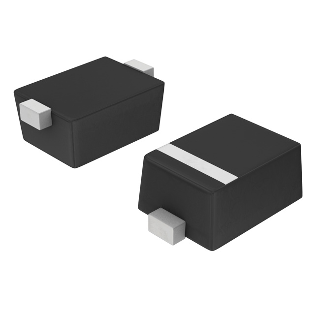
| Package Case | SOD-923 | Digi-Key | |
| Power Line Protection | No | Digi-Key | |
| Power Peak Pulse | - | Digi-Key | |
| Supplier Device Package | SOD-923 | Digi-Key | |
| Type | Zener | Digi-Key | |
| Unidirectional Channels | 1 | Digi-Key | |
| Voltage Clamping Max Ipp | 9.8V | Digi-Key | |
| Voltage Reverse Standoff (Typ) | 5V (Max) | Digi-Key |
When To Use
Use the ESD9L5.0ST5G in general-purpose transient voltage suppression applications where a breakdown voltage minimum of 5.4V and a reverse standoff voltage of 5V (Max) are suitable. It is ideal for protecting sensitive circuits from ESD and surge events with peak pulse currents up to 1A (8/20µs). Avoid using this device in power line protection applications, as it does not support power line protection requirements. For higher voltage or power line protection needs, select a device specifically rated for those conditions.
When Not To Use
-
High-current power rails >1A peak surge: The 1A peak pulse rating limits transient energy absorption. Use a high-current synchronous buck with external FETs for robust surge handling and improved efficiency.
-
Low-voltage linear regulator dropout stage (<1V differential): The 5.4V breakdown and 5V reverse standoff make this part unsuitable for tight dropout conditions. Use an LDO regulator for low noise and minimal input-to-output voltage differential.
-
Battery-powered sensor with μA sleep currents: No quiescent current spec or optimization for low leakage. Use a low-IQ PFM buck to maximize battery life and prevent premature drain.
Application Notes
The ESD9L5.0ST5G should be placed as close as possible to the protected node to minimize the loop area and reduce inductive effects during transient events. The cathode (Zener diode) terminal is the noise-sensitive node and must be routed carefully to the circuit ground to avoid noise coupling. Due to its low power rating and peak pulse current of 1A, no heatsink is required under normal operating conditions within the specified temperature range of -55°C to 150°C (TJ). Surface mount on a SOD-923 footprint for optimal thermal and electrical performance.
Gotchas
-
[Derating ignored at high temperature]: Engineers often assume the 1A peak pulse rating applies across the full -55°C to 150°C range. In reality, pulse current capability derates with temperature rise, risking thermal runaway under repeated surges.
Fix: Verify transient thermal impedance at maximum TJ and derate surge current accordingly in worst-case ambient. -
[Capacitance impact on high-speed signals underestimated]: The 0.5pF capacitance is typical at 1MHz but rises at higher frequencies, causing unexpected signal attenuation or ringing on GHz data lines.
Fix: Measure insertion loss at target frequency and consider adding series resistors or alternate protection strategies if distortion exceeds spec. -
[Improper polarity during assembly]: The unidirectional nature means reversed orientation results in no clamping and potential device damage during ESD events, which can appear as intermittent failures.
Fix: Include polarity marking verification steps in assembly and inspection protocols. -
[Close proximity to switching nodes]: Placing the device too close to high dV/dt switching nodes can couple noise into sensitive protected lines through PCB parasitics, triggering false clamp events or jitter.
Fix: Physically separate the device from high-frequency switching nodes and use ground planes to shield sensitive signals.