Key Specs
| Spec | Value | Condition | Source |
|---|---|---|---|
| Current Continuous Drain ID 25 C | 37A (Tc) | Digi-Key | |
| Drain-source Voltage (Max) | 650 V | Digi-Key | |
| Drive Voltage Max RDS On Min RDS On | 15V | Digi-Key | |
| FET Feature | - | Digi-Key | |
| FET Type | N-Channel | Digi-Key | |
| Gate Charge Qg Max VGS | 46 nC @ 15 V | Digi-Key | |
| Gate-source Voltage (Max) | +15V, -4V | Digi-Key | |
| Grade | - | Digi-Key | |
| Input Capacitance Ciss Max VDS | 1020 pF @ 600 V | Digi-Key | |
| Mounting Type | Through Hole | Digi-Key | |
| Operating Temperature Range | -40°C ~ 175°C (TJ) | Digi-Key | |
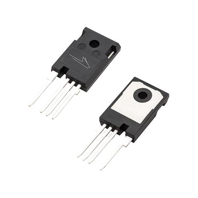
| Package Case | TO-247-4 | Digi-Key | |
| Power Dissipation (Max) | 150W (Tc) | Digi-Key | |
| Qualification | - | Digi-Key | |
| RDS On Max ID VGS | 79mOhm @ 13.2A, 15V | Digi-Key | |
| Supplier Device Package | TO-247-4L | Digi-Key | |
| Technology | SiCFET (Silicon Carbide) | Digi-Key | |
| VGS Th Max ID | 3.6V @ 5mA | Digi-Key |
When To Use
-
650 V DC bus → 24 V @ 30 A: The 650 V drain-source voltage rating provides ample margin for high-voltage DC bus rails, while the 37 A continuous drain current at 25°C ensures handling of 30 A load without thermal runaway. Using a lower-voltage MOSFET risks avalanche breakdown during bus transients or switching overshoot.
-
Industrial motor drive inverter stage: The SiC technology and 79 mΩ RDS(on) at 13.2 A and 15 V gate drive enable efficient switching at high voltages with minimal conduction losses. Choosing a silicon MOSFET would increase switching losses and risk latch-up due to slower switching and higher junction temperatures.
-
High-frequency isolated power supply primary switch: The low total gate charge of 46 nC at 15 V allows for faster gate switching with less driver loss, critical at switching frequencies above 100 kHz in TO-247-4 packages. A device with higher gate charge would cause excessive gate driver heating and slow switching transitions, increasing EMI and switching losses.
When Not To Use
-
Output current > 37 A continuous: The 37 A continuous drain current limit disqualifies this device for loads exceeding that current. Use a multi-phase buck controller to parallel multiple FETs and share current while keeping junction temperature in check.
-
Low dropout linear regulation (<1 V differential): The relatively high RDS(on) and switching nature make this unsuitable for low-voltage linear regulation where noise and dropout are critical. Use an LDO regulator instead to maintain low noise and precise output voltage with minimal dropout.
-
Quiescent current critical battery-powered sensor: The datasheet does not specify ultra-low gate leakage or quiescent current suitable for μA-level standby current. Use a low-IQ PFM buck controller designed for minimal quiescent current in sleep modes.
Application Notes
-
The switching node (SW) must have a compact layout with minimized loop area to reduce EMI and ringing, especially due to the fast switching of the SiC channel.
-
the Gate pin and the Source pin are noise-sensitive; ensure gate drive traces are short and use a low-inductance Kelvin source connection to improve gate voltage accuracy and reduce false turn-on.
-
Guard rings or ground pours around the gate driver and source pins help suppress high-frequency switching noise coupling into the gate drive.
-
The TO-247-4 package has a dedicated Kelvin source pin (pin 3) separate from the main source tab; connect this Kelvin source directly to the gate driver return for accurate gate drive voltage sensing.
-
Avoid routing high-current source or drain traces near the gate drive signals to prevent gate voltage jitter and potential shoot-through.
Pin numbers are package-specific. Verify against the datasheet pinout diagram before routing.
Gotchas
-
[Ignoring maximum gate-source voltage polarity]: The gate-source voltage max is +15 V and -4 V. Applying negative gate voltage beyond -4 V (e.g., from bootstrap or negative spikes) can cause gate oxide damage, resulting in sudden device failure or erratic switching. Measure gate voltage with a differential probe and clamp negative gate swings using a zener diode or resistor clamp.
-
[Assuming RDS(on) at 25°C applies at full junction temperature]: The 79 mΩ RDS(on) is specified at 25°C and 13.2 A; at elevated junction temperatures near 175°C, RDS(on) can increase significantly, causing thermal runaway if not derated. Use thermal imaging or junction temperature estimates and derate current accordingly.
-
[Neglecting gate charge impact on gate driver]: The 46 nC gate charge at 15 V requires a robust gate driver capable of sourcing/sinking sufficient current at the intended switching frequency; otherwise, slow gate transitions cause increased switching losses and EMI. Validate driver capability with gate waveform measurements and use dedicated SiC gate drivers or gate buffers.
-
[Using common source tab as gate drive return]: The TO-247-4 package includes a Kelvin source pin for gate drive reference; connecting gate drive return to the main source tab instead introduces inductance and noise, causing erratic switching or false turn-on. Always route the gate driver return to the Kelvin source pin (pin 3) exclusively.