A89103KEVSR-3 vs 2ED2106S06FXUMA1: Gate Driver IC Comparison for Power Electronics Engineers
Quick verdict
For three-phase motor drive or multi-phase MOSFET gate driving with a wide supply voltage range and automotive-grade qualification, the A89103KEVSR-3 is the better choice due to its integrated three drivers, floating configuration, and extended 4.5V to 85V supply. For simpler two-channel high-side/low-side applications requiring faster switching and stronger peak drive current within a limited 10V–20V supply, the 2ED2106S06FXUMA1 offers superior switching speed and higher peak current capability.
Spec comparison table
| Spec | A89103KEVSR-3 | 2ED2106S06FXUMA1 | Notes |
|---|---|---|---|
| Channel Type | 3-Phase | Independent | A89103KEVSR-3 integrates 3 drivers for 3-phase systems; 2ED2106S06FXUMA1 is 2 independent drivers. |
| Current Peak Output (Source/Sink) | Not specified | 290mA / 700mA | 2ED2106S06FXUMA1 offers explicit high peak current, useful for fast switching of large gates. |
| Driven Configuration | Floating | High-Side, Low-Side | A89103KEVSR-3 supports floating gate drive, critical for bootstrap or isolated half-bridge topologies. |
| Gate Type | N-Channel MOSFET | IGBT, N-Channel MOSFET | 2ED2106S06FXUMA1 supports both IGBT and MOSFET, offering more versatility in device choice. |
| Grade | Automotive | Not specified | A89103KEVSR-3 is AEC-Q100 qualified, critical for automotive reliability. |
| Input Type | Non-Inverting | CMOS, TTL | 2ED2106S06FXUMA1 accepts both CMOS and TTL logic levels, slightly more flexible. |
| Logic Voltage (V_IL, V_IH) | 0.8V / 2V | 1.1V / 1.7V | A89103KEVSR-3 has lower logic input thresholds, better for lower voltage control logic. |
| Mounting Type | Surface Mount, Wettable Flank | Surface Mount | Both surface mount; wettable flanks on A89103KEVSR-3 help with optical inspection and solder reliability. |
| Number of Drivers | 3 | 2 | A89103KEVSR-3 reduces component count for 3-phase systems. |
| Operating Temperature Range | -40°C to 150°C (TA) | -40°C to 125°C (TA) | A89103KEVSR-3 supports higher ambient temperatures, better for harsh environments. |
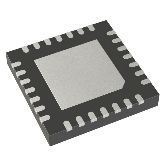
| Package Case | 28-VFQFN Exposed Pad | 8-SOIC (0.154”, 3.90mm Width) | A89103KEVSR-3’s thermal pad improves heat dissipation; 2ED2106S06FXUMA1 is smaller but less thermally optimized. |
| Qualification | AEC-Q100 | Not specified | Automotive qualification only on A89103KEVSR-3. |
| Rise/Fall Time (typical) | 1.2µs / 150ns | 100ns / 35ns | 2ED2106S06FXUMA1 switches significantly faster, beneficial for high-frequency operation. |
| Voltage Supply | 4.5V to 85V | 10V to 20V | A89103KEVSR-3 supports a much wider supply voltage range, enabling more flexible system architectures. |
| Supplier Device Package | 28-QFN (6x6) | PG-DSO-8-69 | Different package types, affecting PCB layout and thermal design. |
| High-Side Voltage Max Bootstrap | N/A | 650V | 2ED2106S06FXUMA1 supports bootstrap voltages up to 650V, suitable for high-voltage half-bridge designs. |
Design trade-offs
The A89103KEVSR-3 targets three-phase systems requiring floating gate drivers and a wide supply voltage range. Its 4.5V to 85V supply allows operation in higher-voltage motor drives or industrial systems without additional level shifting or specialized power rails. The integrated triple driver reduces BOM and PCB space, especially important in compact automotive or industrial motor controllers. The exposed pad VFQFN package aids in thermal dissipation, which is critical given the wider operating temperature range up to 150°C ambient.
However, the A89103KEVSR-3’s typical rise time (1.2µs) is much slower than the 2ED2106S06FXUMA1, which can limit switching frequency or increase switching losses in high-speed applications. Its unspecified peak output current means designers must be cautious driving large gate charge MOSFETs at high frequency.
In contrast, the 2ED2106S06FXUMA1 provides explicit peak source/sink currents of 290mA and 700mA, enabling rapid charging/discharging of MOSFET or IGBT gates. This translates to faster switching transitions (100ns rise, 35ns fall) and lower switching losses, beneficial in high-frequency or high-efficiency designs. The narrower operating voltage range (10V–20V) and bootstrap voltage rating up to 650V make it suited for standard half-bridge topologies with bootstrap supply.
Thermally, the 2ED2106S06FXUMA1’s small SOIC package limits heat dissipation and may require careful layout and possibly derating at high ambient temperatures, especially with frequent switching cycles. The lack of automotive qualification reduces confidence in harsh environments, making it less suitable for automotive or rugged industrial applications.
Layout-wise, the A89103KEVSR-3’s floating driver architecture demands careful isolation and routing of floating grounds and bootstrap supplies, increasing PCB complexity. The 2ED2106S06FXUMA1’s independent high-side/low-side drivers simplify layout but require separate bootstrap arrangements and careful gate drive sequencing.
Cost at volume is not explicitly detailed here but generally, integrated multi-channel ICs like the A89103KEVSR-3 tend to have higher unit cost but lower overall system cost due to fewer components, while simpler dual-channel drivers like the 2ED2106S06FXUMA1 may be less expensive per unit but require additional external components.
Use-case fit
Choose A89103KEVSR-3 when…
- Designing three-phase BLDC or PMSM motor drives requiring integrated triple drivers in a single package.
- Operating in automotive or harsh industrial environments needing AEC-Q100 qualification and extended temperature range to 150°C.
- Systems with supply voltages varying broadly from 4.5V up to 85V, minimizing external power rail complexity.
- Applications where floating driver topology is mandatory to drive high-side MOSFETs in half-bridge or full-bridge configurations.
- PCB space optimization is critical but thermal dissipation must be maintained via exposed pad QFN packages.
Choose 2ED2106S06FXUMA1 when…
- Driving two independent MOSFET or IGBT gates in a high-side/low-side half-bridge configuration.
- High switching speed and peak gate drive current are necessary to minimize switching losses (100ns rise, 700mA peak sink).
- Operating supply voltage is strictly between 10V and 20V, common in standard gate drive rails.
- The system is less demanding on automotive qualification or extended temperature, e.g., consumer or general industrial applications.
- Smaller PCB footprint in SOIC package is desired and thermal dissipation can be managed through layout or cooling.
Drop-in compatibility
These two devices are not pin-compatible or footprint-compatible. The A89103KEVSR-3 uses a 28-pin VFQFN package with wettable flanks and an exposed thermal pad, designed for three integrated drivers with floating configurations. The 2ED2106S06FXUMA1 comes in an 8-pin SOIC package suitable for two independent drivers in high-side/low-side configuration.
Substituting one for the other would require significant PCB redesign, including routing changes, power supply adjustments, and likely firmware changes to handle different input logic thresholds and driver configurations.
Alternatives to consider
- IR2110 (International Rectifier): A classic high-voltage high-side/low-side driver supporting bootstrap voltages up to 500V, widely used with proven robustness.
- UCC37322 (Texas Instruments): A dual high-speed MOSFET driver with high peak current (~9A), suited for high-frequency switching applications.
- MIC4605 (Microchip): A dual high-side/low-side driver with integrated deadtime and built-in protections, suitable for industrial motor drives.