Key Specs
| Spec | Value | Condition | Source |
|---|---|---|---|
| Applications | - | Digi-Key | |
| Function | Controller - Commutation, Direction Management | Digi-Key | |
| Grade | Automotive | Digi-Key | |
| Interface | PWM | Digi-Key | |
| Motor Type AC DC | Brushless DC (BLDC) | Digi-Key | |
| Motor Type Stepper | - | Digi-Key | |
| Mounting Type | Surface Mount | Digi-Key | |
| Operating Temperature Range | -40°C ~ 150°C (TA) | Digi-Key | |
| Output Configuration | Pre-Driver - Half Bridge (3) | Digi-Key | |
| Output Current (Max) | - | Digi-Key | |
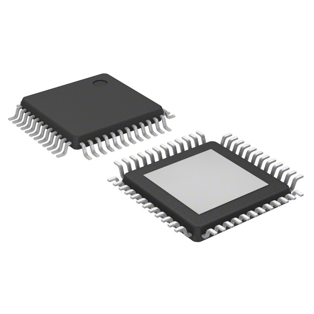
| Package Case | 48-LQFP Exposed Pad | Digi-Key | |
| Step Resolution | - | Digi-Key | |
| Supplier Device Package | 48-LQFP-EP (7x7) | Digi-Key | |
| Technology | Power MOSFET | Digi-Key | |
| Voltage Load | 5.5V ~ 50V | Digi-Key | |
| Voltage Supply | 3V ~ 5.5V | Digi-Key |
When To Use
Use the A4935KJPTR-T in automotive brushless DC motor control applications requiring integrated half-bridge pre-driver functionality, operating within a voltage supply range of 3 V to 5.5 V and load voltage range of 5.5 V to 50 V. It is ideal where a surface-mount package (48-LQFP-EP) and a PWM interface are needed for direction management and commutation control. Avoid using this device in stepper motor control applications or in systems requiring output current ratings beyond the integrated MOSFET capability; in those cases, consider dedicated stepper motor drivers or higher current discrete MOSFET solutions.
When Not To Use
-
High current (>10A) motor phases: Current capability is limited by internal power MOSFETs and package thermal dissipation. For loads exceeding this, use a high-current synchronous buck with external FETs that can handle higher current with external device scaling.
-
Systems requiring switching frequencies above 500kHz: This part is designed for typical BLDC commutation frequencies; if switching above 500kHz is required for inductor size reduction, use a high-frequency buck controller specialized for high-frequency operation.
-
Applications needing galvanic isolation between control and power domains: The integrated half-bridge driver lacks isolation features. Use an isolated flyback controller to maintain electrical isolation and prevent ground loop issues.
Application Notes
The half-bridge output nodes switch rapidly and require minimizing the loop area to reduce EMI and switching losses. Pay particular attention to the exposed pad and ground connections for thermal dissipation; although the device can operate up to 150°C ambient, a proper PCB thermal design is necessary to avoid overheating at high load conditions. The PWM input pin is noise-sensitive; use proper filtering and routing to prevent false triggering. A heatsink is generally not required when the device is mounted on a PCB with adequate copper area for heat dissipation at typical operating points.
Gotchas
-
Connecting the device outside the specified supply voltage range (3 V to 5.5 V) can cause malfunction or permanent damage. Always verify supply voltage before operation to avoid device failure.
-
Improper PCB layout resulting in a large switching loop area at the half-bridge output nodes can cause excessive EMI and reduced efficiency. Minimize loop area by placing the device close to the load and using a solid ground plane.